AT90S2313
58
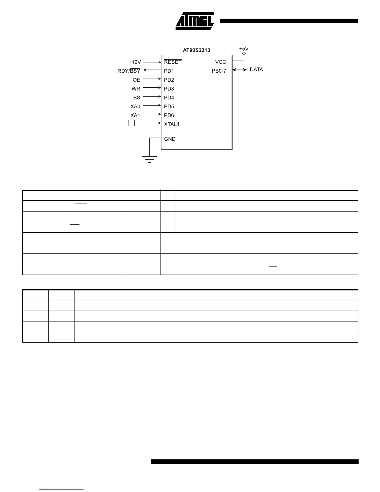
Figure 49. Parallel Programming
.
Table 23. Pin Name Mapping
Signal Name in Programming Mode Pin Name I/O Function
RDY/BSY PD1 O 0: Device is busy programming, 1: Device is ready for new command
OE
PD2 I Output Enable (Active low)
WR
PD3 I Write Pulse (Active low)
BS PD4 I Byte Select (‘0’ selects low byte, ‘1’ selects high byte)
XA0 PD5 I XTAL Action Bit 0
XA1 PD6 I XTAL Action Bit 1
DATA PB7-0 I/O Bidirectional Databus (Output when OE
is low)
Table 24. XA1 and XA0 Coding
XA1 XA0 Action when XTAL1 is Pulsed
0 0 Load Flash or EEPROM Address (High or low address byte determined by BS)
0 1 Load Data (High or Low data byte for Flash determined by BS)
1 0 Load Command
1 1 No Action, Idle