29
7679H–CAN–08/08
AT90CAN32/64/128
4.5.3 Address Latch Requirements
Due to the high-speed operation of the XRAM interface, the address latch must be selected with
care for system frequencies above 8 MHz @ 4V and 4 MHz @ 2.7V. When operating at condi-
tions above these frequencies, the typical old style 74HC series latch becomes inadequate. The
External Memory Interface is designed in compliance to the 74AHC series latch. However, most
latches can be used as long they comply with the main timing parameters. The main parameters
for the address latch are:
• D to Q propagation delay (t
PD
).
• Data setup time before G low (t
SU
).
• Data (address) hold time after G low (
TH
).
The External Memory Interface is designed to guaranty minimum address hold time after G is
asserted low of t
h
= 5 ns. Refer to t
LAXX_LD
/ t
LLAXX_ST
in Table 26-7 through Table 26-14 of Sec-
tion 26.9 on page 375. The D-to-Q propagation delay (t
PD
) must be taken into consideration
when calculating the access time requirement of the external component. The data setup time
before G low (t
SU
) must not exceed address valid to ALE low (t
AVLLC
) minus PCB wiring delay
(dependent on the capacitive load).
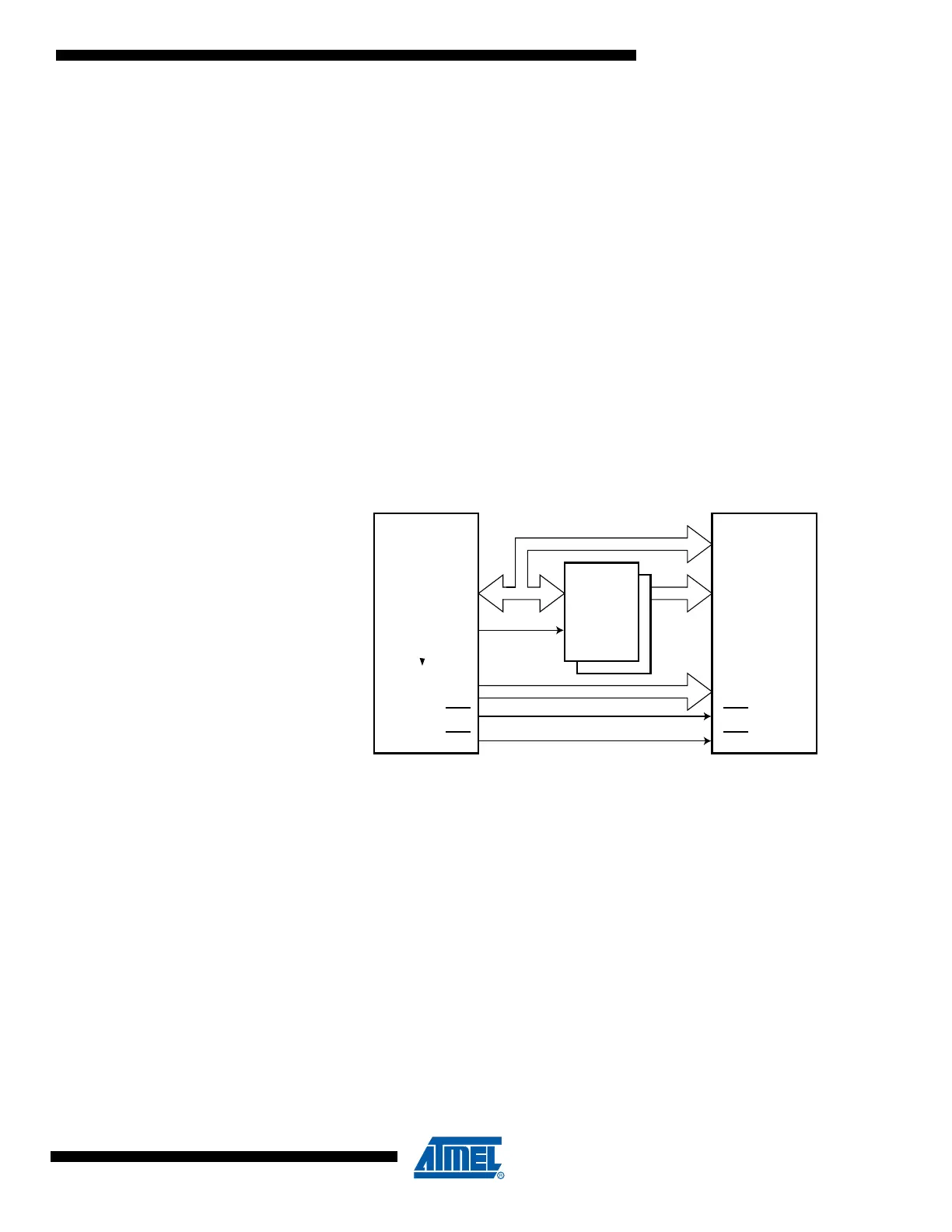
Figure 4-5. External SRAM Connected to the AVR
4.5.4 Pull-up and Bus-keeper
The pull-ups on the AD7:0 ports may be activated if the corresponding Port register is written to
one. To reduce power consumption in sleep mode, it is recommended to disable the pull-ups by
writing the Port register to zero before entering sleep.
The XMEM interface also provides a bus-keeper on the AD7:0 lines. The bus-keeper can be dis-
abled and enabled in software as described in “External Memory Control Register B – XMCRB”
on page 33. When enabled, the bus-keeper will ensure a defined logic level (zero or one) on the
AD7:0 bus when these lines would otherwise be tri-stated by the XMEM interface.
4.5.5 Timing
External Memory devices have different timing requirements. To meet these requirements, the
AT90CAN32/64/128 XMEM interface provides four different wait-states as shown in Table 4-4. It
is important to consider the timing specification of the External Memory device before selecting
the wait-state. The most important parameters are the access time for the external memory
compared to the set-up requirement of the AT90CAN32/64/128. The access time for the Exter-
nal Memory is defined to be the time from receiving the chip select/address until the data of this
D[7:0]
A[7:0]
A[15:8]
RD
WR
SRAM
DQ
G
AD7:0
ALE
A15:8
RD
WR
AVR

 Loading...


