304
7679H–CAN–08/08
AT90CAN32/64/128
• Shift-DR: The Bypass Register cell between TDI and TDO is shifted.
23.5 Boundary-scan Related Register in I/O Memory
23.5.1 MCU Control Register – MCUCR
The MCU Control Register contains control bits for general MCU functions.
• Bits 7 – JTD: JTAG Interface Disable
When this bit is zero, the JTAG interface is enabled if the JTAGEN Fuse is programmed. If this
bit is one, the JTAG interface is disabled. In order to avoid unintentional disabling or enabling of
the JTAG interface, a timed sequence must be followed when changing this bit: The application
software must write this bit to the desired value twice within four cycles to change its value. Note
that this bit must not be altered when using the On-chip Debug system.
If the JTAG interface is left unconnected to other JTAG circuitry, the JTD bit should be set to
one. The reason for this is to avoid static current at the TDO pin in the JTAG interface.
23.5.2 MCU Status Register – MCUSR
The MCU Status Register provides information on which reset source caused an MCU reset.
• Bit 4 – JTRF: JTAG Reset Flag
This bit is set if a reset is being caused by a logic one in the JTAG Reset Register selected by
the JTAG instruction AVR_RESET. This bit is reset by a Power-on Reset, or by writing a logic
zero to the flag.
23.6 Boundary-scan Chain
The Boundary-scan chain has the capability of driving and observing the logic levels on the digi-
tal I/O pins, as well as the boundary between digital and analog logic for analog circuitry having
off-chip connection.
23.6.1 Scanning the Digital Port Pins
Figure 23-3 shows the Boundary-scan Cell for a bi-directional port pin with pull-up function. The
cell consists of a standard Boundary-scan cell for the Pull-up Enable – PUExn – function, and a
bi-directional pin cell that combines the three signals Output Control – OCxn, Output Data –
ODxn, and Input Data – IDxn, into only a two-stage Shift Register. The port and pin indexes are
not used in the following description
The Boundary-scan logic is not included in the figures in the datasheet. Figure 23-4 shows a
simple digital port pin as described in the section “I/O-Ports” on page 66. The Boundary-scan
details from Figure 23-3 replaces the dashed box in Figure 23-4.
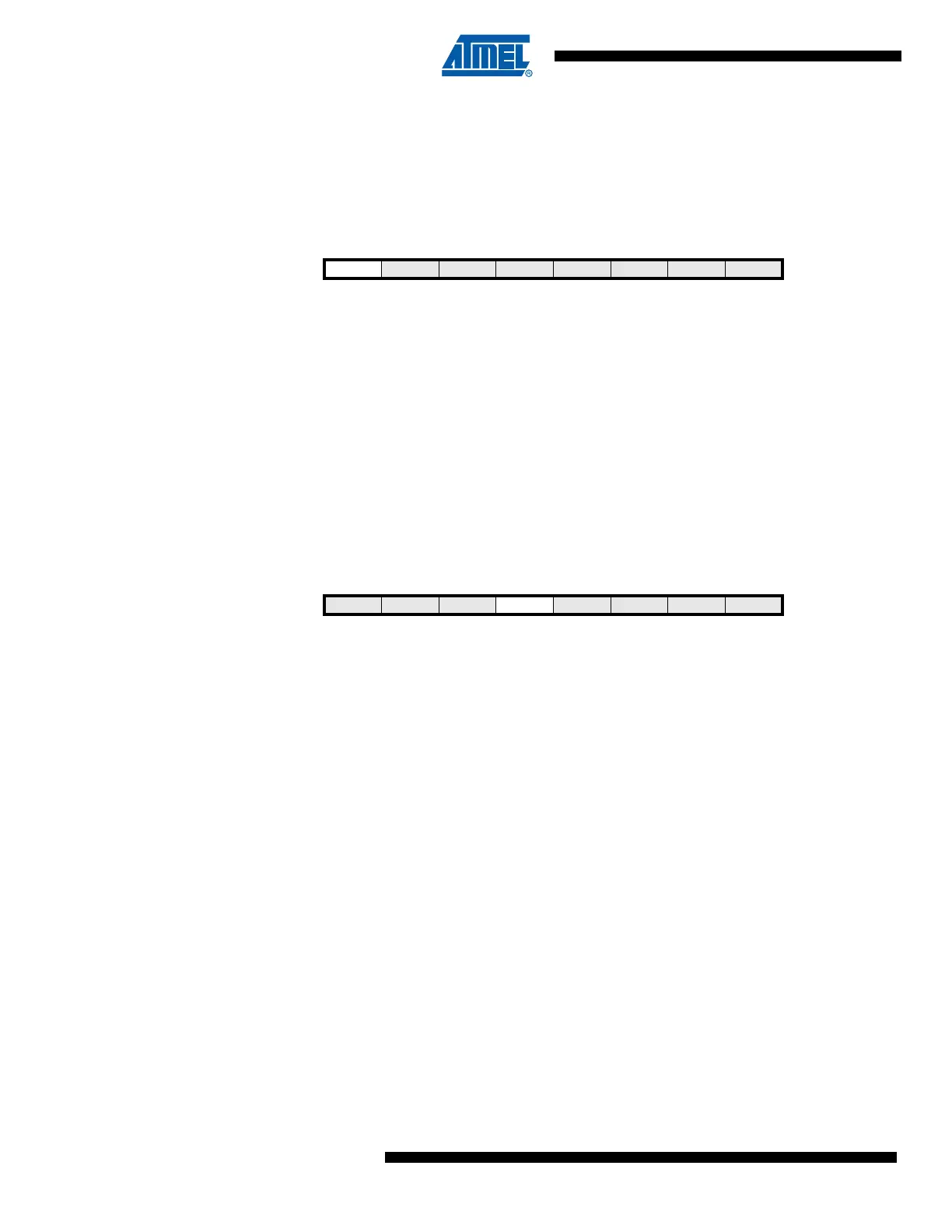
Bit 76543210
JTD
– – PUD – – IVSEL IVCE MCUCR
Read/Write R/W R R R/W R R R/W R/W
Initial Value 0 0 0 0 0 0 0 0
Bit 76543210
– – –JTRFWDRF BORF EXTRF PORF MCUSR
Read/Write R R R R/W R/W R/W R/W R/W
Initial Value 0 0 0 See Bit Description

 Loading...


