306
7679H–CAN–08/08
AT90CAN32/64/128
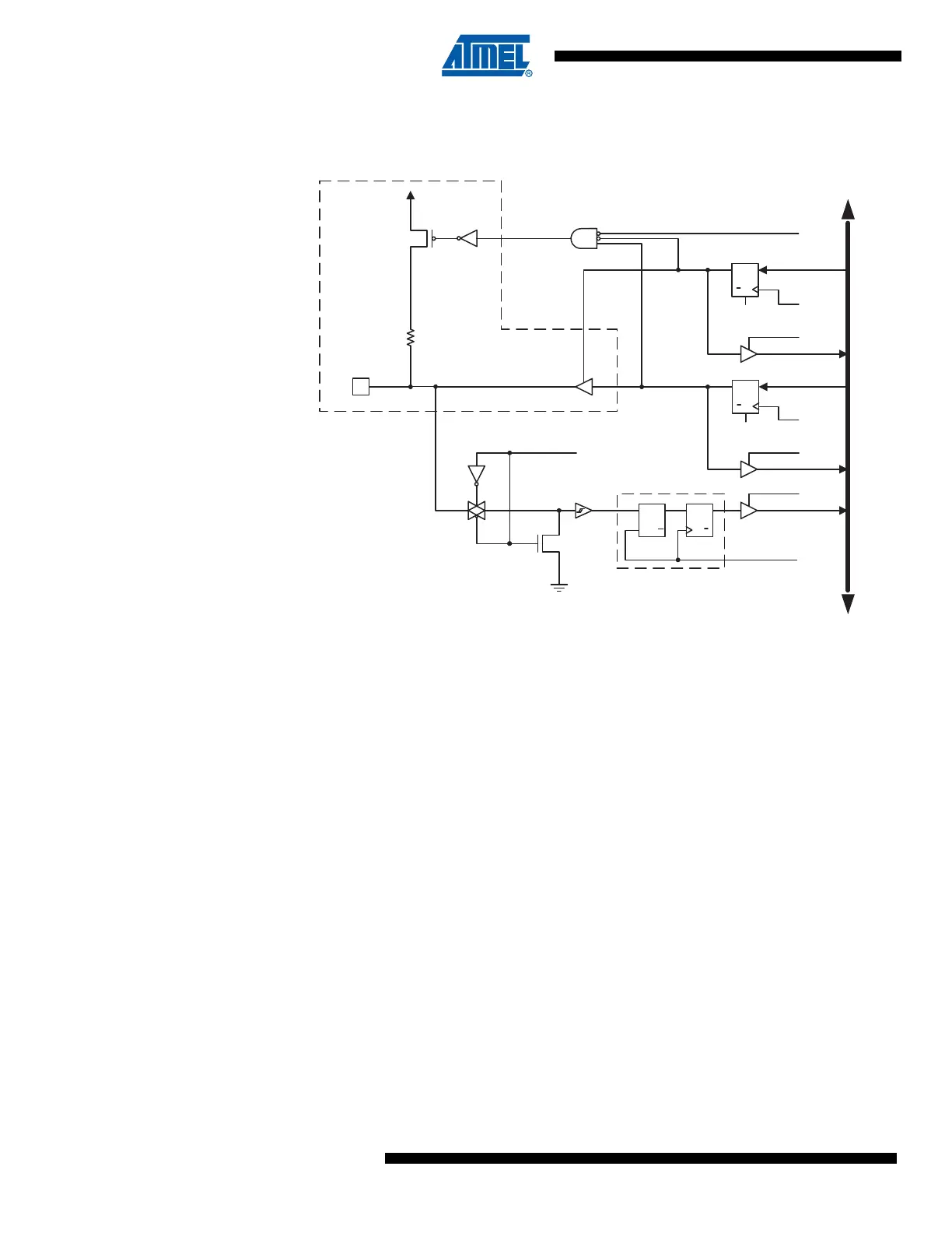
Figure 23-4. General Port Pin Schematic Diagram
23.6.2 Boundary-scan and the Two-wire Interface
The two Two-wire Interface pins SCL and SDA have one additional control signal in the scan-
chain; Two-wire Interface Enable – TWIEN. As shown in Figure 23-5, the TWIEN signal enables
a tri-state buffer with slew-rate control in parallel with the ordinary digital port pins. A general
scan cell as shown in Figure 23-9 is attached to the TWIEN signal.
Notes: 1. A separate scan chain for the 50 ns spike filter on the input is not provided. The ordinary scan
support for digital port pins suffice for connectivity tests. The only reason for having TWIEN in
the scan path, is to be able to disconnect the slew-rate control buffer when doing boundary-
scan.
2. Make sure the OC and TWIEN signals are not asserted simultaneously, as this will lead to
drive contention.
CLK
RPx
RRx
WPx
RDx
WDx
PUD
SYNCHRONIZER
WDx: WRITE DDRx
WPx: WRITE PORTx
RRx: READ PORTx REGISTER
RPx: READ PORTx PIN
PUD: PULLUP DISABLE
CLK : I/O CLOCK
RDx: READ DDRx
D
L
Q
Q
RESET
RESET
Q
Q
D
Q
Q
D
CLR
PORTxn
Q
Q
D
CLR
DDxn
PINxn
DATA BUS
SLEEP
SLEEP: SLEEP CONTROL
Pxn
I/O
I/O
See Boundary-scan
Description for Details!
PUExn
OCxn
ODxn
IDxn
PUExn: PULLUP ENABLE for pin Pxn
OCxn: OUTPUT CONTROL for pin Pxn
ODxn: OUTPUT DATA to pin Pxn
IDxn: INPUT DATA from pin Pxn

 Loading...


