308
7679H–CAN–08/08
AT90CAN32/64/128
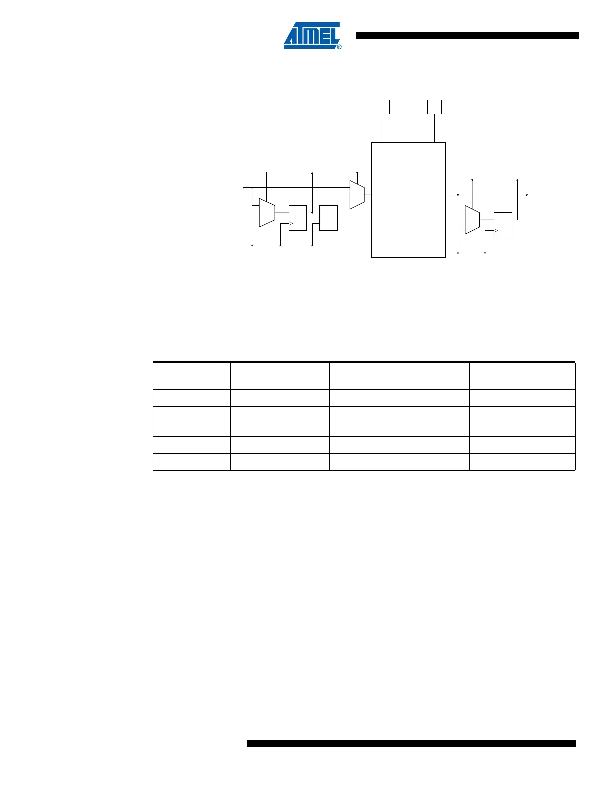
Figure 23-7. Boundary-scan Cells for Oscillators and Clock Options
Table 23-5 summaries the scan registers for the external clock pin XTAL1, oscillators with
XTAL1/XTAL2 connections as well as external Timer2 clock pin TOSC1 and 32kHz Timer2
Oscillator.
Notes: 1. Do not enable more than one clock source as clock at a time.
2. Scanning an Oscillator output gives unpredictable results as there is a frequency drift between
the internal Oscillator and the JTAG TCK clock. If possible, scanning an external clock is
preferred.
3. The main clock configuration is programmed by fuses. As a fuse is not changed run-time, the
main clock configuration is considered fixed for a given application. The user is advised to
scan the same clock option as to be used in the final system. The enable signals are sup-
ported in the scan chain because the system logic can disable clock options in sleep modes,
thereby disconnecting the Oscillator pins from the scan path if not provided.
23.6.5 Scanning the Analog Comparator
The relevant Comparator signals regarding Boundary-scan are shown in Figure 23-8. The
Boundary-scan cell from Figure 23-9 is attached to each of these signals. The signals are
described in Table 23-6.
The Comparator need not be used for pure connectivity testing, since all analog inputs are
shared with a digital port pin as well.
Table 23-5. Scan Signals for the Oscillators
(1)(2)(3)
Enable Signal Scanned Clock Line Clock Option
Scanned Clock Line
when not Used
EXTCLKEN EXTCLK (XTAL1) External Main Clock 0
OSCON OSCCK
External Crystal
External Ceramic Resonator
1
OSC32EN OSC32CK Low Freq. External Crystal 1
TOSKON TOSCK 32 kHz Timer2 Oscillator 1
0
1
DQ
From
Previous
Cell
ClockDR
ShiftDR
To
Next
Cell
To System Logic
FF1
0
1
DQ DQ
G
0
1
From
Previous
Cell
ClockDR UpdateDR
ShiftDR
To
Next
Cell EXTEST
From Digital Logic
XTAL1 / TOSC1 XTAL2 / TOSC2
Oscillator
ENABLE OUTPUT

 Loading...


