73
7679H–CAN–08/08
AT90CAN32/64/128
The following subsections shortly describe the alternate functions for each port, and relate the
overriding signals to the alternate function. Refer to the alternate function description for further
details.
9.3.1 MCU Control Register – MCUCR
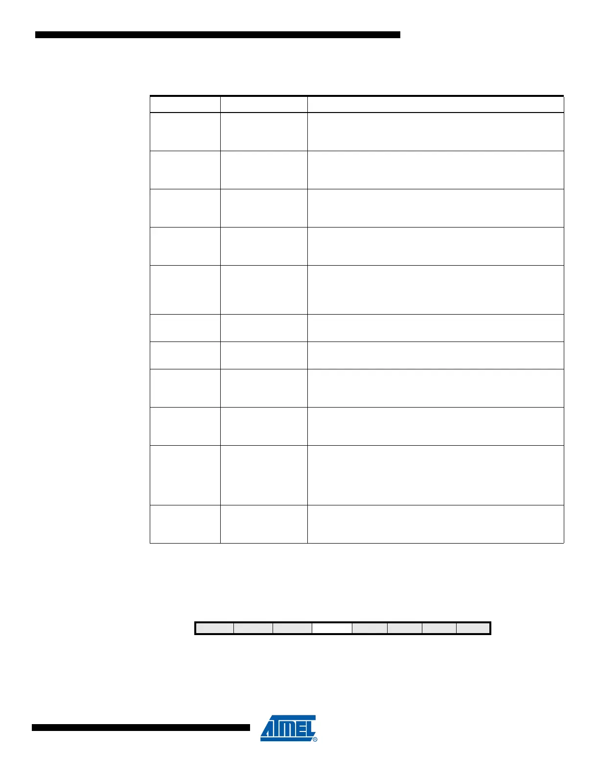
Table 9-2. Generic Description of Overriding Signals for Alternate Functions
Signal Name Full Name Description
PUOE
Pull-up Override
Enable
If this signal is set, the pull-up enable is controlled by the PUOV
signal. If this signal is cleared, the pull-up is enabled when
{DDxn, PORTxn, PUD} = 0b010.
PUOV
Pull-up Override
Value
If PUOE is set, the pull-up is enabled/disabled when PUOV is
set/cleared, regardless of the setting of the DDxn, PORTxn,
and PUD Register bits.
DDOE
Data Direction
Override Enable
If this signal is set, the Output Driver Enable is controlled by the
DDOV signal. If this signal is cleared, the Output driver is
enabled by the DDxn Register bit.
DDOV
Data Direction
Override Value
If DDOE is set, the Output Driver is enabled/disabled when
DDOV is set/cleared, regardless of the setting of the DDxn
Register bit.
PVOE
Port Value
Override Enable
If this signal is set and the Output Driver is enabled, the port
value is controlled by the PVOV signal. If PVOE is cleared, and
the Output Driver is enabled, the port Value is controlled by the
PORTxn Register bit.
PVOV
Port Value
Override Value
If PVOE is set, the port value is set to PVOV, regardless of the
setting of the PORTxn Register bit.
PTOE
Port Toggle
Override Enable
If PTOE is set, the PORTxn Register bit is inverted.
DIEOE
Digital Input
Enable Override
Enable
If this bit is set, the Digital Input Enable is controlled by the
DIEOV signal. If this signal is cleared, the Digital Input Enable
is determined by MCU state (Normal mode, sleep mode).
DIEOV
Digital Input
Enable Override
Value
If DIEOE is set, the Digital Input is enabled/disabled when
DIEOV is set/cleared, regardless of the MCU state (Normal
mode, sleep mode).
DI Digital Input
This is the Digital Input to alternate functions. In the figure, the
signal is connected to the output of the schmitt trigger but
before the synchronizer. Unless the Digital Input is used as a
clock source, the module with the alternate function will use its
own synchronizer.
AIO
Analog
Input/Output
This is the Analog Input/output to/from alternate functions. The
signal is connected directly to the pad, and can be used bi-
directionally.
Bit 7 6 5 4 3 2 1 0
JTD – –PUD– – IVSEL IVCE MCUCR
Read/Write R/W R R R/W R R R/W R/W
Initial Value 0 0 0 0 0 0 0 0

 Loading...


