ATtiny15L
57
Note: 1. “Max” means the highest value where the pin is guaranteed to be read as low
2. “Min” means the lowest value where the pin is guaranteed to be read as high
3. Although each I/O port can sink more than the test conditions (20 mA at V
CC
= 5V, 10 mA at V
CC
= 3V) under steady state
conditions (non-transient), the following must be observed:
1] The sum of all I
OL
, for all ports, should not exceed 100 mA
If I
OL
exceeds the test condition, V
OL
may exceed the related specification.
Pins are not guaranteed to sink current greater than the listed test conditions.
4. Although each I/O port can source more than the test conditions (3 mA at V
CC
= 5V, 1.5 mA at V
CC
= 3V) under steady state
conditions (non-transient), the following must be observed:
1] The sum of all I
OH
, for all ports, should not exceed 100 mA
If I
OH
exceeds the test condition, V
OH
may exceed the related specification. Pins are not guaranteed to source current
greater than the listed test condition.
5. Minimum V
CC
for Power-down is 1.5V. (Only with BOD disabled.)
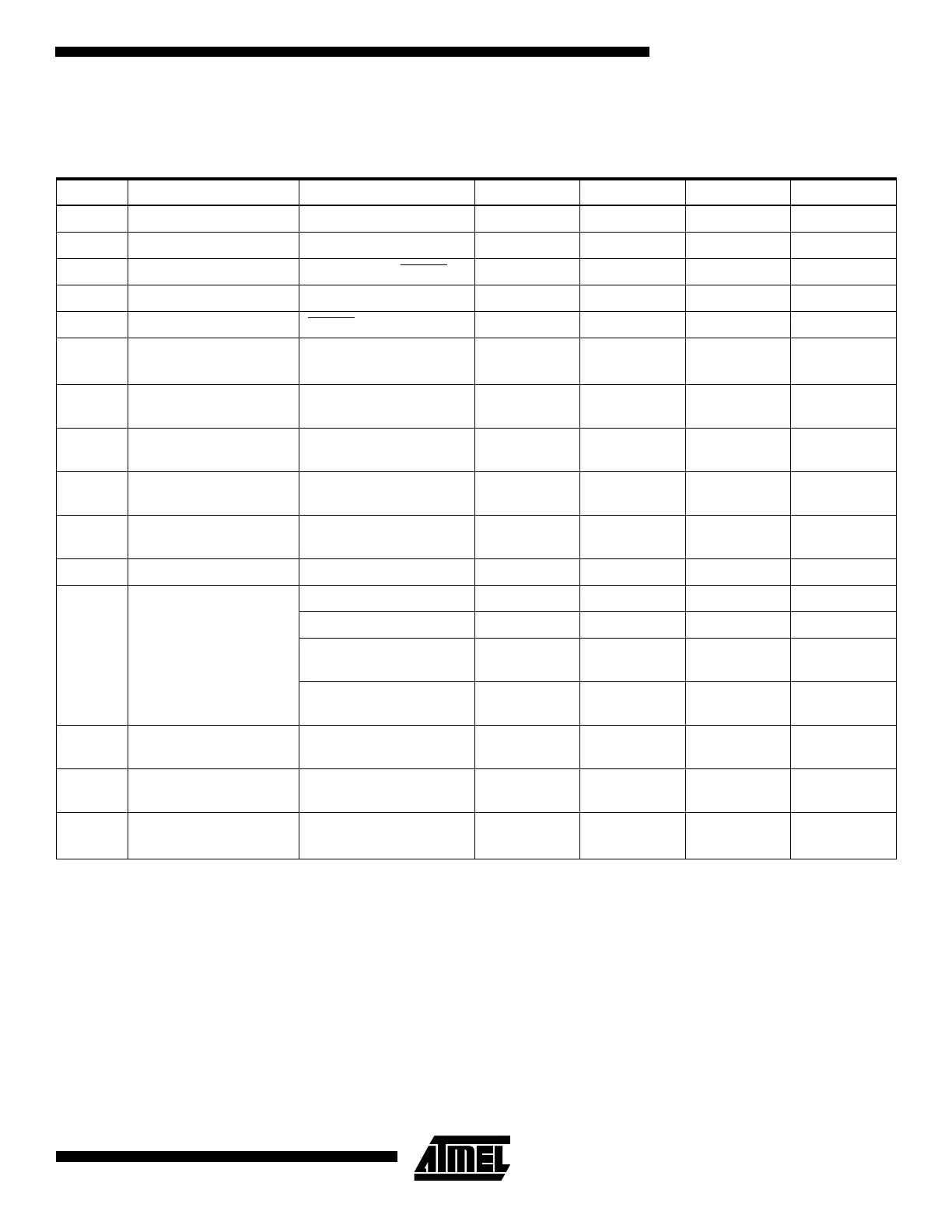
DC Characteristics – Preliminary Data
T
A
= -40°C to 85°C, V
CC
= 2.7V to 5.5V
Symbol Parameter Condition Min Typ Max Units
V
IL
Input Low Voltage Except (XTAL) -0.5 0.3 V
CC
(1)
V
V
IL1
Input Low Voltage XTAL -0.5 0.1 V
CC
(1)
V
V
IH
Input High Voltage Except (XTAL, RESET) 0.6 V
CC
(2)
V
CC
+ 0.5 V
V
IH1
Input High Voltage XTAL 0.7 V
CC
(2)
V
CC
+ 0.5 V
V
IH2
Input High Voltage RESET 0.85 V
CC
(2)
V
CC
+ 0.5 V
V
OL
Output Low Voltage
(1)
Port B
I
OL
= 20 mA, V
CC
= 5V
I
OL
= 10 mA, V
CC
= 3V
0.6
0.5
V
V
V
OL
Output Low Voltage
PB5
I
OL
= 12 mA, V
CC
= 5V
I
OL
= 6 mA, V
CC
= 3V
0.6
0.5
V
V
V
OH
Output High Voltage
(4)
Port B
I
OH
= -3 mA, V
CC
= 5V
I
OH
= -1.5 mA, V
CC
= 3V
4.3
2.3
V
V
I
IL
Input Leakage Current
I/O Pin
V
CC
= 5.5V, Pin Low
(Absolute value)
8.0 µA
I
IH
Input Leakage Current
I/O Pin
V
CC
= 5.5V, Pin High
(Absolute value)
8.0 µA
R
I/O
I/O Pin Pull-up 35 122 kΩ
I
CC
Power Supply Current
Active, V
CC
= 3V 3.0 mA
Idle, V
CC
= 3V 1.0 1.2 mA
Power-down
(2)
, V
CC
= 3V
WDT enabled
9.0 15 µA
Power-down
(2)
, V
CC
= 3V
WDT disabled
<1 2 µA
V
ACIO
Analog Comparator
Input Offset Voltage
V
CC
= 5V
V
IN
= V
CC
/2
40 mV
I
ACLK
Analog Comparator
Input Leakage Current
V
CC
= 5V
V
IN
= V
CC
/2
-50 50 nA
T
ACID
Analog Comparator
Initialization Delay
V
CC
= 2.7V
V
CC
= 4.0V
750
500
ns
 Loading...


