2
8068C–AVR–06/08
XMEGA A3
1. Ordering Information
Notes: 1. This device can also be supplied in wafer form. Please contact your local Atmel sales office for detailed ordering information.
2. Pb-free packaging, complies to the European Directive for Restriction of Hazardous Substances (RoHS directive). Also Halide free and fully Green.
3. For packaging information, see ”Packaging information” on page 63.
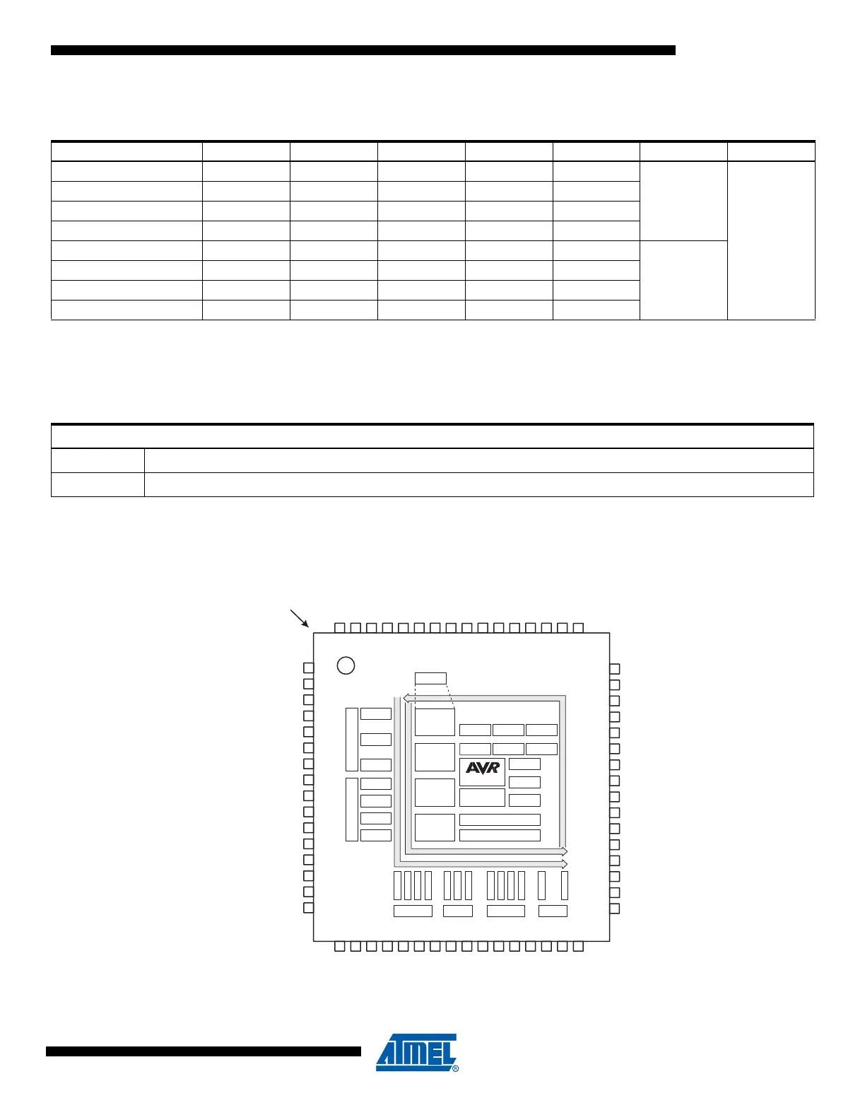
2. Pinout/Block Diagram
Figure 2-1. Block diagram and TQFP-pinout.
Note: 1. For full details on pinout and alternate pin functions refer to ”Pinout and Pin Functions” on page 48.
Ordering Code Flash (B) E
2
(B) SRAM (B) Speed (MHz) Power Supply Package
(1)(2)(3)
Temp
ATxmega256A3-AU 256K + 8K 4K 16K 32 1.8 - 3.6V
64A
-40° - 85°C
ATxmega192A3-AU 192K + 8K 4K 16K 32 1.8 - 3.6V
ATxmega128A3-AU 128K + 8K 2K 8K 32 1.8 - 3.6V
ATxmega64A3-AU 64K + 4K 2K 4K 32 1.8 - 3.6V
ATxmega256A3-MU 256K + 8K 4K 16K 32 1.8 - 3.6V
64M1
ATxmega192A3-MU 192K + 8K 4K 16K 32 1.8 - 3.6V
ATxmega128A3-MU 128K + 8K 2K 8K 32 1.8 - 3.6V
ATxmega64A3-MU 64K + 4K 2K 4K 32 1.8 - 3.6V
Package Type
64A
64-lead, 14 x 14 mm Body Size, 1.0 mm Body Thickness, 0.8 mm Lead Pitch, Thin Profile Plastic Quad Flat Package (TQFP)
64M1
64-pad, 9 x 9 x 1.0 mm Body, Lead Pitch 0.50 mm, 5.40 mm Exposed Pad, Micro Lead Frame Package (MLF)
INDEX CORNER
17
18
19
20
21
22
23
24
25
26
27
28
29
30
31
32
64
63
62
61
60
59
58
57
56
55
54
53
52
51
50
49
48
47
46
45
44
43
42
41
40
39
38
37
36
35
34
33
1
2
3
4
5
6
7
8
9
10
11
12
13
14
15
16
PF2
PF1
PF0
VCC
GND
PE7
PE6
PE5
PE4
PE3
PE2
PE1
PE0
VCC
GND
PD7
PA3
PA4
PA5
PA6
PA7
PB0
PB1
PB2
PB3
PB4
PB5
PB6
PB7
GND
VCC
PC0
PC1
PC2
PC3
PC4
PC5
PC6
PC7
GND
VCC
PD0
PD1
PD2
PD3
PD4
PD5
PD6
PA2
PA1
PA0
AVCC
GND
PR1
PR0
RESET/PDI_CLK
PDI_DATA
PF7
PF6
VCC
GND
PF5
PF4
PF3
FLASH
RAM
E
2
PROM
DMA
Interrupt Controller
OCD
ADC A
ADC B
DAC B
AC A0
AC A1
AC B0
AC B1
Por
t
A
Por t
B
Event System ctrl
Por t R
Power
Control
Reset
Control
Watchdog
OSC/CLK
Control
BOD POR
RTC
EVENT ROUTING NETWORK
DATA BU S
DATA BU S
VREF
TEMP
Port C Port D Port E Port F
CPU
T/C0:1
USART0:1
SPI
TWI
T/C0:1
USART0:1
SPI
T/C0:1
USART0:1
SPI
TWI
T/C0
USART0