41
8068C–AVR–06/08
XMEGA A3
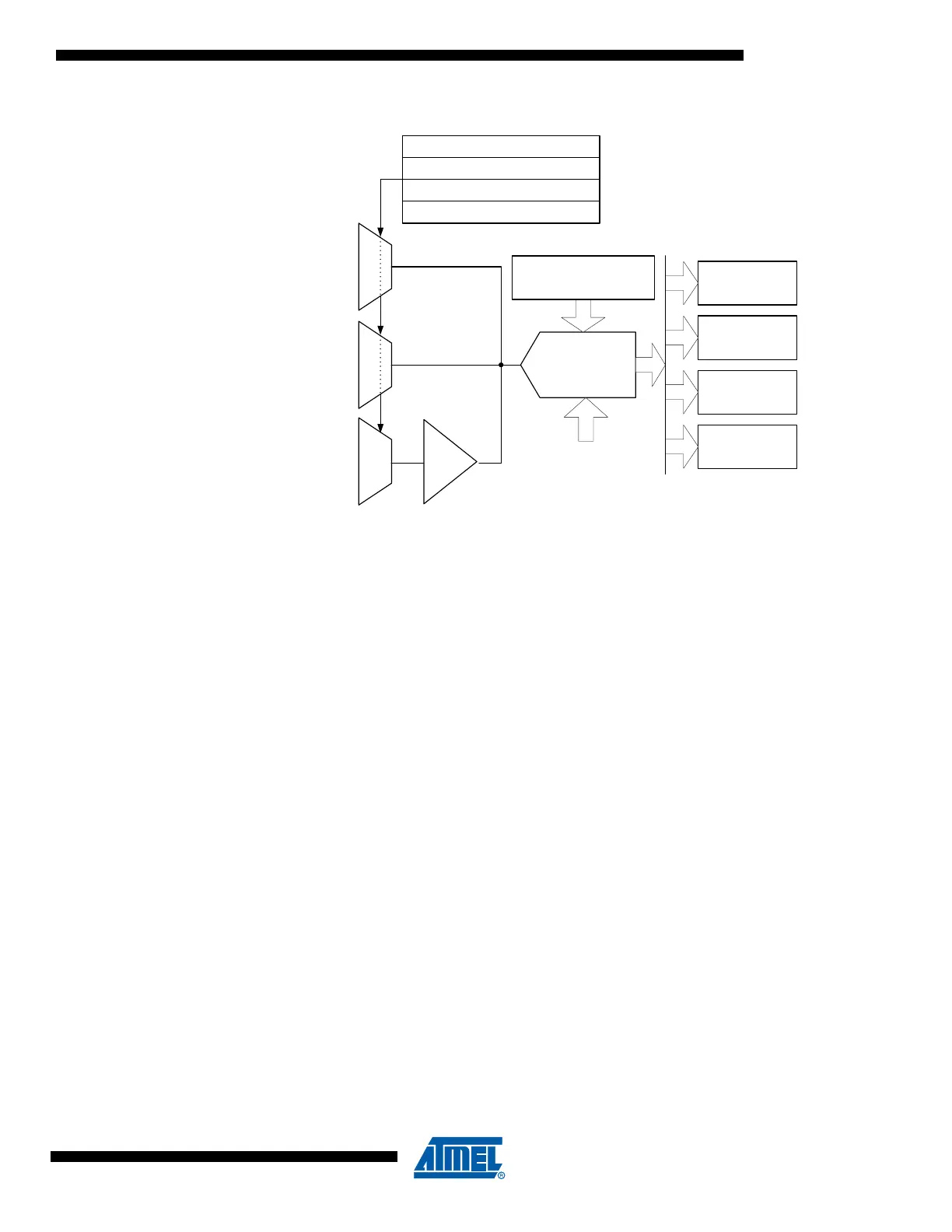
Figure 24-1. ADC overview
Each ADC has four MUX selection registers with a corresponding result register. This means
that four channels can be sampled within 1.5 µs without any intervention by the application other
than starting the conversion. The results will be available in the result registers.
The ADC may be configured for 8- or 12-bit result, reducing the minimum conversion time (prop-
agation delay) from 3.5 µs for 12-bit to 2.5 µs for 8-bit result.
ADC conversion results are provided left- or right adjusted with optional ‘1’ or ‘0’ padding. This
eases calculation when the result is represented as a signed integer (signed 16-bit number).
PORTA and PORTB each has one ADC. Notation of these peripherals are ADCA and ADCB,
respectively.
ADC
Channel A
Register
Channel B
Register
Channel C
Register
Channel D
Register
Pin inputsPin inputs
1-64 X
Internal inputs
Channel A MUX selection
Channel B MUX selection
Channel C MUX selection
Channel D MUX selection
Event
Trigger
Configuration
Reference selection

 Loading...