13
A product detector is used to demodulate all signals, with an envelope detector used to generate AGC
control voltage. The noise blanker employs a separate noise pulse receiver to provide raw blanking pulses
which are manipulated in the main processor to form effective blanking pulses on the noise blanker gate.
There is a great deal of commonality between receive and transmit paths in both the R.F. and audio circuits.
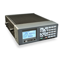
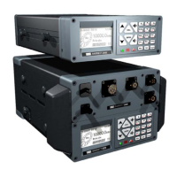
Power amplifier PCB
The PA PCB raises the power level from the RF section of the microprocessor board, to 10 W, 25 W, or 125
W PEP depending on the power setting or whether the transceiver is mated with the 2040 manpack
adaptor.
Seven low pass filters provide harmonic rejection over the full frequency range, reduce receiver LO
radiation and enhance image rejection in the receiver. The PA PCB also contains the power protection
circuitry guarding against over-voltage, and reverse voltage supplies.
A VSWR bridge generates representative voltages for forwards and reverse power measurements which
tell the DSP the condition of the PA’s load. From these two signals the DSP sets the power of the PA. DSP
either sets the PEP or to reduces overall power in the event of a bad load.