Technical Information on On-board Flash Programmer FP-40 Aug. 31, 2023 (Second edition)
5
Pin
No.
Signal
Output
*1
Pin
No.
Signal
Output
*1
7 SWDIO
8 GND
*1: Input/output is denoted for the target system.
*2: External input/output function signal that will be at VTref level when high.
This signal is not connected to the target (CPU).
*3: Unused. NC.
*4: 3.3V External input/output function signal. This signal is not connected to
the target (CPU).
*5: Power supply function signal.
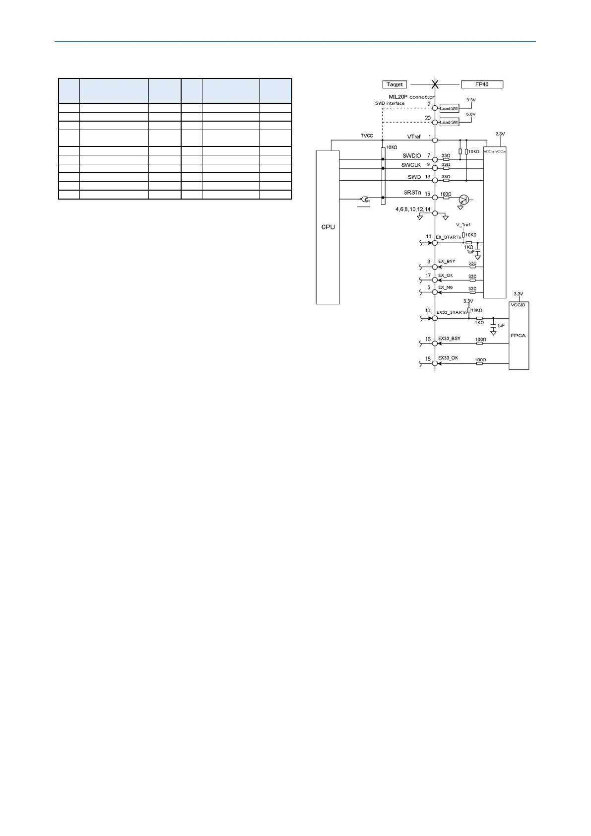
Target connection reference diagram
To prevent malfunction, the length of wirings from the CPU to the target connector should be kept as short as possible.
If the waveform disturbance exceeds the device specifications, suppress the disturbance by inserting a damping resistor into the signal line or use
other means.