Technical Information on On-board Flash Programmer FP-40 Aug. 31, 2023 (Second edition)
7
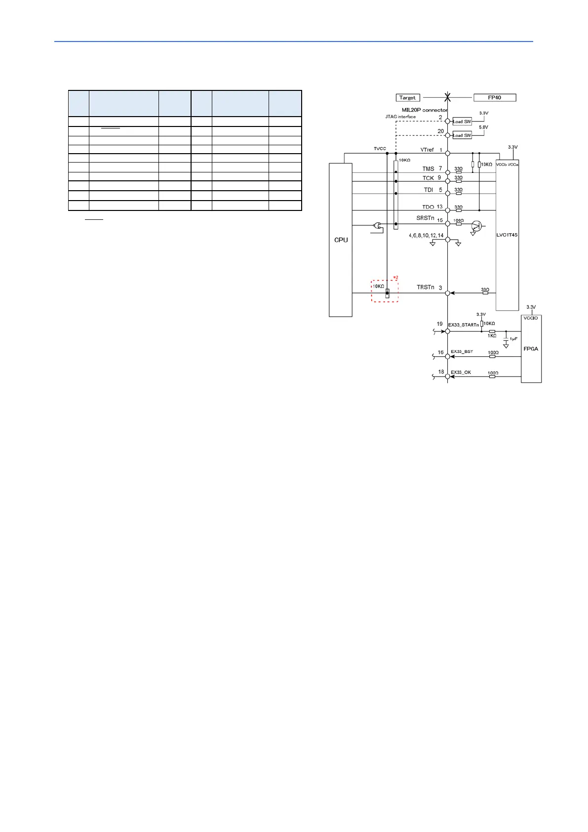
Target connection reference diagram
Pin
No.
Signal
Output
*1
Pin
No.
Signal
Output
*1
*1: Input/output denoted is for the target system.
*2:
TRST TRST is not used with Cortex-M core CPUs. Leave as NC. For other
CPUs, please refer to the datasheet of the CPU to be connected.
Please note that CPUs that require connection may require the signals to
be pulled-down.
Note that some CPUs manufactured by Renesas Electronics require some
precautions. Refer to "Reference:RZ/A and RZ/T series /SRST, /TRST
reference diagram" below.
*3: 3.3V External input/output function signal. This signal is not connected to
the target (CPU).
*4: Power supply function signal.
*5: Reserved for FP-40's own usage, leave as NC.
To prevent malfunction, the length of wirings from the CPU to the target connector should be kept as short as possible.
If the waveform disturbance exceeds the device specifications, suppress the disturbance by inserting a damping resistor into the signal line or use
other means.