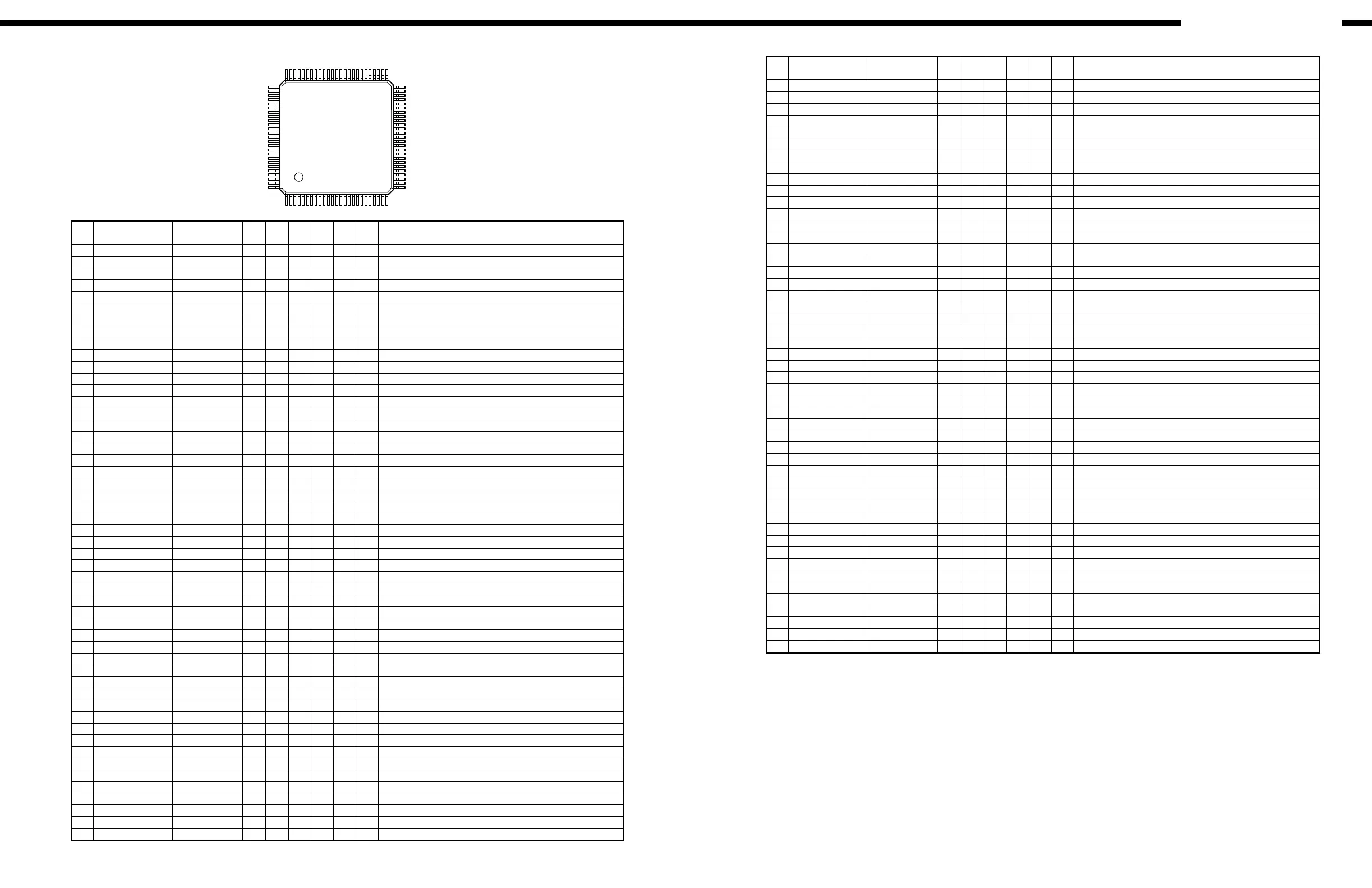
TMP95FY64F (IC801)
TMP95FY64F Terminal Function
Pin.
No.
Name
1 VREFL VREFL
A/D ref. GND
2 AVss AVss
A/D GND
3 AVcc AVcc
AD +5V
4 DAOUT0 DAOUT0 No connection
5 DAOUT1 DAOUT1 O C
Od L L No connection
6 _NMI _NMI I
Not used (fixed to H)
7 P53/_BUSRQ ASIC RESET O N
Eu H H ASIC control terminal (L: Reset)
8 P54/_BUSAK WP1 O C
Od Memory write protect for DSP1
9 P55/_WAIT WP2 O C
Od Memory write protect for DSP2
10 P56/INT0 B.DOWN I
E
↓
&L Eu Z
Power down detect (L: Detected)
11 P57/SCLK2/_CTS2 ROM_RES1 O C
Od Memory reset for DSP1
12 P80/TxD0 MISO O C MAIN-SUB
µ
com comm. control terminal (Data out)
13 P81/RxD0 MOSI I
MAIN-SUB
µ
com comm. control terminal (Data in)
14 P82/SCLK0/_CTS0 CLK I/O C MAIN-SUB
µ
com comm. control terminal (I2C clock in/out)
15 P83/TxD1 DIR MOSI O C
Z L DIR control terminal (LC89055Q), control data output
16 P84/RxD1 DIR MISO I
Lv
DIR control input terminal (LC89055Q), control data input
17 P85/SCLK1/_CTS1 DIR CLK O C
Z L DIR control terminal (LC89055Q), control clock output
18 P86/TxD2 TxD O C
Z L Data send output to external (common with 1394 data comm.)
19 P87/RxD2 RxD I
Lv
Data receive input from external (common with 1394 data comm.)
20 P60/_CS0 D.EXP OE O C
Z L Port Expander control out for DIGITAL input switching (TC4094B)
21 P61/_CS1 D.EXP CLK O C
Z L Port Expander control out for DIGITAL input switching (TC4094B)
22 P62/_CS2 D.EXP DATA O C
Z L Port Expander control out for DIGITAL input switching (TC4094B)
23 P63/_CS3 D.EXP STB O C
Z L Port Expander control out for DIGITAL input switching (TC4094B)
24 CLK CLK O C
Eu
25 Vcc Vcc
+5V
26 Vss I/O1
GND
27 X1 Xin I
X'tal connection
28 X2 Xout O
X'tal connection
29 _EA _EA
Fixed to +5V
30 _RESET RESET I
Lv Eu L
Reset input
31 P70/TI0/INT1 DSP ACK1 I
E
↑
&L
DSP1 host interface comm. respond input (L: OK)
32 P71/TO1 _DSP1 RESET O C
Od L L DSP1 reset output terminal (L: Reset)
33 P72/TO3/INT2 AC-3 RF DET. I
E
↓
&L
AC-3 RF signal detect input (L: AC-3 RF signal input)
34 P73/TI4/INT3 DAC-192 O C
Sets D/A to 192k
35 P74/TO5 _DSP2 RESET O C
Od L L DSP2 reset output terminal (L: Reset)
36 P75/TO7/INT4 _REQ O C
Eu H L MAIN-SUB
µ
com comm. control terminal (L: Comm. request from SUB)
37 P90/TI8/INT5 _ACK I
E
↓
&L Eu
MAIN-SUB
µ
com comm. control terminal (L: Ack. return from MAIN)
38 P91/TI9/INT6 CSI I
Lv
DIR control input terminal (LC89055Q), L: PCM
39 P92/TO8 EMP I
Lv
H: EMP ON
40 P93/TO9 DEEPM O C
Ed L L
41 P94/TIA/INT7 _CS I
E
↑
&L Od
DIR control input terminal (LC89055Q), L
→
H: Cannel status change
42 P95/TIB/INT8 ERR I
E
↑
&L
DIR control input terminal (LC89055Q), H: ERR
43 P96/TOA/TOB DIR RESET O C
Z L DIR control input terminal (LC89055Q), L: Reset
44 Vcc Vcc
+5V
45 P00/D0 DIT_RESET C
Z L DIT control terminal
46 P01/D1 DIT CLK C
Z L DIT control terminal
47 P02/D2 DIT uDATA C
Z L DIT control terminal
48 P03/D3 DIT ST C
Z L DIT control terminal
49 P04/D4 DIT_CS C
Z L DIT control terminal
50 P05/D5 DIT R/W C
Z L DIT control terminal
51 P06/D6 DH/RESET C
Z L DHIVA board reset (fixed to L)
Symbol I/O Type Det Op Res Ini Function
Pin.
No.
Name Symbol I/O Type Det Op Res Ini Function
52 P07/D7 DMUTE C
Z L Digital input MUTE control output (same control as SELCK)
53 P10/D8 I/O1 I/O C
Z L DSP comm. terminal (ADSP21061L:D16)
54 P11/D9 I/O2 I/O C
Z L DSP comm. terminal (ADSP21061L:D17)
55 P12/D10 I/O3 I/O C
Z L DSP comm. terminal (ADSP21061L:D18)
56 P13/D11 I/O4 I/O C
Z L DSP comm. terminal (ADSP21061L:D19)
57 P14/D12 I/O5 I/O C
Z L DSP comm. terminal (ADSP21061L:D20)
58 P15/D13 I/O6 I/O C
Z L DSP comm. terminal (ADSP21061L:D21)
59 P16/D14 I/O7 I/O C
Z L DSP comm. terminal (ADSP21061L:D22)
60 P17/D15 I/O8 I/O C
Z L DSP comm. terminal (ADSP21061L:D23)
61 AM8/_16 Fixed to +5V
62 Vss Vss
GND
63 Vcc Vcc
+5V
64 P27/A23 _DSP REQUEST1 O C
ZL
DSP1 (ADSP21061L-A:IRQ 1_) host interface interrupt req. output, L: REQ
65 P26/A22 WRITE1 O C
Z L DSP1 comm. control terminal (H: DATA WRITE)
66 P25/A21 _DSP REQUEST2 O C
ZL
DSP2 (ADSP21061L-A:IRQ 1_) host interface interrupt req. output, L: REQ
67 P24/A20 WRITE2 O C
Z L DSP2 comm. control terminal (H: DATA WRITE)
68 P23/A19 DSP ACK2 I
E
↑
&L
DSP2 host interface comm. respond input (L: OK)
69 P22/A18 BUSY2 I
Lv
DSP busy check flag (ADSP21061L-B:FLAG 2B) input, L: Normal
70 P21/A17 FLAG 3A I
Lv
Special flag for ROM update (ADSP21061L-A:FLAG 3A)
71 P20/A16 BUSY1 I
Lv
DSP busy check flag (ADSP21061L-A:FLAG 2A) input, L: Normal
72 P37/A15 SEL CK O C
Z L ADC/DIR data/clock switching control terminal (L: ADC)
73 P36/A14 DIR CE O C
Z L DIR control terminal (LC89055Q), control chip enable output
74 P35/A13 FLAG 3B I
Lv
Special flag for ROM update (ADSP21061L-A:FLAG 3B)
75 P34/A12 DAC-RESET2 O C
Od L H DAC control terminal (L: Power down,
↑
: Reset, H: Normal)
76 P33/A11 DIGITAL POWER O C
Z L DIGITAL power ON/OFF switching
77 P32/A10 DIR AUTO O C
Od Z L
78 P31/A9 BPSYNC O C
ZL
79 P30/_B00T/A8 _B00T I
Lv Eu Z
Single Chip/Single Boot switching input (H & Reset: Single Chip Mode)
80 P47/A7 _DEMOD RESET O C
Od L L Demodulator reset output (L: Reset)
81 P46/A6 DEMOD ON O C
Od L L Demodulator osc. control output (H: Osc.)
82 P45/A5 FGAIN O C
Z L IV AMP GAIN switching control output (L: Sub-woofer on)
83 P44/A4 A/D RESET O N
Eu H H A/D control terminal (L: Reset)
84 P43/A3 DAC-RESET1 O C
Od L H DAC control terminal (L: Power down,
↑
: Reset, H: Normal)
85 P42/A2 DAC-DIF. DAC differential use: H
86 P41/A1 DIG. (AC3) MUTE O C
Od Z L Digital mute control output (L: AC-3 or DTS decode possible)
87 P40/A0 ERR MUTE_ O C
Od L L Pop noise preventive mute control output
88 P50/_RD DH IN O C
Z L For 1394 (fixed to L)
89 P51/_WR DH OUT O C
Z L For 1394 (fixed to L)
90 P52/_HWR ROM_RES2 O C
Od Memory reset for DSP2
91 Vss Vss
GND
92 PA0/AN0 96K DET I
Lv
96k signal detect input, H: 96k
93 PA1/AN1 DHERR I
Lv
DHIVA board error input (fixed to L)
94 PA2/AN2 I
Lv
Not used (Pull down)
95 PA3/AN3/_ADTRG Not used (Pull down)
96 PA4/AN4 I
Lv
Not used (Pull down)
97 PA5/AN5 I
Lv
Not used (Pull down)
98 PA6/AN6 I
Lv
Not used (Pull down)
99 PA7/AN7 MODE-0-SUB I
Lv
FLASH ROM rewrite mode input
100 VREFH VREFH
AD ref. +5V
Note: Pin No. : Terminal number of microcomputer.
Port Name : The name entered in the data sheet of microcomputer.
Symbol : Symbolized interface function.
I/O : Input or out of part.
“I” = Input port
“O” = Output port
Type : Composition of port in case of output port.
“C” = CMOS output
“N” = NMOS open drain output
“P” = PMOS open drain output
Op : Pull up/Pull down selection information.
“Iu” = Inner microcomputer pull up
“Id” = Inner microcomputer pull down
“Eu” = External microcomputer pull up
“Ed” = External microcomputer pull down
Det : Indicates judging state of input port. Level detection is “LV”; Edge detection is “Ed”; Detection by both shifting is “E&L”; Serial data
detection is “S” (Serial data output is also “S”).
Res : State at reset.
“H” = Outputs High Level at reset
“L” = Outputs Low Level at reset
“Z” = Becomes High impedance mode at reset
Ini : Initial output state.
Function : Function and logical level explanation of signals to be interface.
15
AVR-4802/AVC-A11SR
3TMP95FY64F.p65 01/08/02, 20:58Page 2-3 AdobePageMaker6.5J/Win
 Loading...