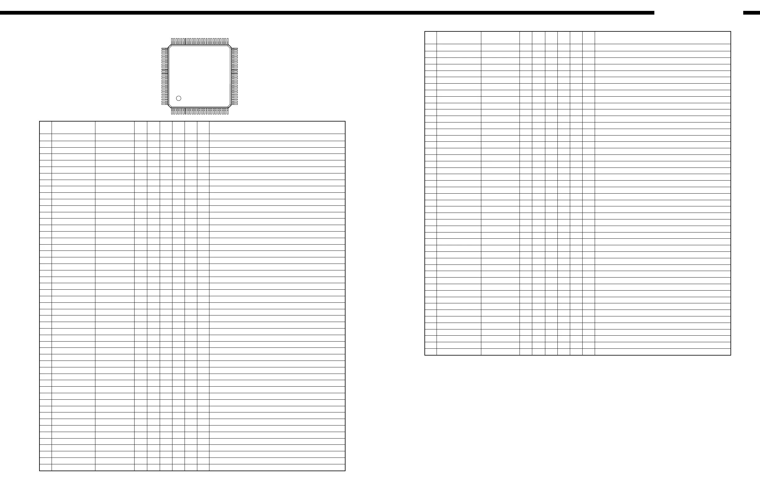
TMP95FY64F (IC802)
TMP95FY64F Terminal Function
Pin.
No.
Name Symbol I/O Type Det Op Res Ini Function
1 VREFL VREFL
A/D ref. GND
2 AVss AVss
A/D GND
3 AVcc AVcc
AD +5V
4 DAOUT0 DAOUT0 O
No connection
5 DAOUT1 DAOUT1 O
No connection
6 _NMI _NMI I
Not used (fixed to H)
7 P53/_BUSRQ ACK O C
Z
MAIN-SUB
µ
com comm. control terminal
8 P54/_BUSAK REQ I
Lv Eu Z
MAIN-SUB
µ
com comm. control terminal
9 P55/_WAIT PLFL DATA O C
Z L PLL & FL control terminal (LC72131 & LC7511NE)
10 P56/INT0 PROTECT I
E
↑
&L Ed Z
Protection detect input (H: Detected)
11 P57/SCLK2/_CTS2 PLFL CLK O C
Z L PLL & FL control terminal (LC72131 & LC7511NE)
12 P80/TxD0 PLL STB O C
Z L PLL control terminal (LC72131)
13 P81/RxD0 ERROR LED O C
Ed Z H Not used
14 P82/SCLK0/_CTS0
MULTI ROOM POWER
OC
Z L Power amp control terminal for MULTI ROOM (H: ON)
15 P83/TxD1 MOSI O C
Z L MAIN-SUB
µ
com comm. control terminal
16 P84/RxD1 MISO I
Lv
Z
MAIN-SUB
µ
com comm. control terminal
17 P85/SCLK1/_CTS1 CLK I/O (C)
Z
MAIN-SUB
µ
com comm. control terminal
18 P86/TxD2 TxD O C
Z L Data transfer terminal to external
19 P87/RxD2 RxD I
Lv
Z
Data receive terminal from external
20 P60/_CS0 FUNC/TONE CLK O C
Z L Clock output for Function switching/Tone IC control
21 P61/_CS1 FUNC/TONE DATA O C
Z L Data output for Function switching/Tone IC control
22 P62/_CS2 ST/MONO O C
Z L Stereo/Mono control signal (L: Stereo receive)
23 P63/_CS3 STANDBY O C
Ed Z H Standby LED drive output (H: Light)
24 CLK CLK O C
No connection
25 Vcc Vcc
+5V
26 Vss Vss
GND
27 X1 X1 I
X'tal connection
28 X2 X2 O
X'tal connection
29 _EA _EA I
Fixed to +5V
30 _RESET _RESET I
Lv Iu L
Reset input
31 P70/TI0/INT1 VIDEO POWER O C
Z L Video power ON/OFF switching (H: ON)
32 P71/TO1 DIGITAL POWER O C
Z L Digital power ON/OFF switching (H: ON)
33 P72/TO3/INT2 (VKK POWER) O
Z L Not used (-VKK power ON/OFF switching)
34 P73/TI4/INT3 SEL A (M) I
Lv Eu Z
Master VR turn detect input (Rotary encoder)
35 P74/TO5 SEL B (M) I
Lv Eu Z
Master VR turn detect input (Rotary encoder)
36 P75/TO7/INT4 (FAN CONTROL) O C
Z L Not used (Fan control for power Tr)
37 P90/TI8/INT5 B.DOWN I
E
↓
&L Eu Z
Power down detect (L: Detected)
38 P91/TI9/INT6 STEREO I
Lv Eu Z
Stereo detect (L: Received)
39 P92/TO8 TUNED I
Lv Eu Z
Tune detect (L: Tuned)
40 P93/TO9 S MONI.DET I
Lv Eu Z
S Monitor connection detect input (L: Connected)
41 P94/TIA/INT7 REMOCON I
E
↑
&L Ed Z
Remote control signal input
42 P95/TIB/INT8 S SIG.DET I
Lv Eu Z
S signal detect input (H: Signal input)
43 P96/TOA/TOB SYNC.DET I
Lv Eu Z
Sync. detect input (H: External sync.)
44 Vcc Vcc
+5V
45 P00/D0 POWER O C
Z H Power relay control output (H: ON)
46 P01/D1 V.EXP OE O C
Z L Port expander control output for video circuit (TC4094B)
47 P02/D2 V.EXP CLK O C
Z L Port expander control output for video circuit (TC4094B)
48 P03/D3 V.EXP DATA O C
Z L Port expander control output for video circuit (TC4094B)
49 P04/D4 V.EXP STB O C
Z L Port expander control output for video circuit (TC4094B)
50 P05/D5 SP.EXP OE O C
Z L Port expander control output for speaker output (TC4094B)
51 P06/D6 SP.EXP CLK O C
Z L Port expander control output for speaker output (TC4094B)
52 P07/D7 SP.EXP DATA O C
Z L Port expander control output for speaker output (TC4094B)
Pin.
No.
Name Symbol I/O Type Det Op Res Ini Function
53 P10/D8 SP.EXP STB O C
Z L Port expander control output for speaker output (TC4094B)
54 P11/D9 A.EXP OE O C
Z L Port expander control output for audio mute and relay control (TC4094B)
55 P12/D10 A.EXP CLK O C
Z L Port expander control output for audio mute and relay control (TC4094B)
56 P13/D11 A.EXP DATA O C
Z L Port expander control output for audio mute and relay control (TC4094B)
57 P14/D12 A.EXP STB O C
Z L Port expander control output for audio mute and relay control (TC4094B)
58 P15/D13 MAIN/SUB O C
Z L RS232C/MAIN-SUB
µ
com input switching
59 P16/D14 RESET2 O C
Z L SUB
µ
com reset output
60 P17/D15 E.VOL STBB O C
Z L E VR control output (TC9459)
61 AM8/_16 AM8/_16
I
Fixed to +5V
62 Vss Vss
GND
63 Vcc Vcc
+5V
64 P27/A23 STB EXP OE O C
Z H Port expander control output for audio circuit IC strobe (TC4094B)
65 P26/A22 STB EXP CLK O C
Z L Port expander control output for audio circuit IC strobe (TC4094B)
66 P25/A21 STB EXP DATA O C
Z L Port expander control output for audio circuit IC strobe (TC4094B)
67 P24/A20 STB EXP STB O C
Z H Port expander control output for audio circuit IC strobe (TC4094B)
68 P23/A19 LED CLK O C
Z L LED driver control output (M66313)
69 P22/A18 LED DATA O C
Z L LED driver control output (M66313)
70 P21/A17 LED LE O C
Eu Z L LED driver control output (M66313)
71 P20/A16 LED OE O C
Z H LED driver control output (M66313)
72 P37/A15 SEL H (T) I
Lv Eu Z
Treble VR turn detect input (Rotary encoder)
73 P36/A14 SEL G (T) I
Lv Eu Z
Treble VR turn detect input (Rotary encoder)
74 P35/A13 SEL F (B) I
Lv Eu Z
Bass VR turn detect input (Rotary encoder)
75 P34/A12 SEL E (B) I
Lv Eu Z
Bass VR turn detect input (Rotary encoder)
76 P33/A11 SEL D (I) I
Lv Eu Z
Input selector turn detect input (Rotary encoder)
77 P32/A10 SEL C (I) I
Lv Eu Z
Input selector turn detect input (Rotary encoder)
78 P31/A9 H/P DET I
Lv Eu Z
H/P detect input (H: Detected)
79 P30/_BOOT/A8 _BOOT I
Lv Eu Z
Single Chip/Single Boot switching input (H & Reset: Single Chip Mode)
80 P47/A7 E.VOL CLK O C
Z L E VR control output (TC9459)
81 P46/A6 E.VOL DATA O C
Z L E VR control output (TC9459)
82 P45/A5 E.VOL STBA O C
Z L E VR control output (TC9459)
83 P44/A4 E.VOL MULTI STB O C
Z L E VR control output for MULTI ROOM (TC9459)
84 P43/A3 O C
Z L No connection
85 P42/A2 OSD RST O C
Z H OSD control terminal (M35015)
86 P41/A1 OSD STB O C
Z H OSD control terminal (M35015)
87 P40/A0 OSD DATA O C
Z L OSD control terminal (M35015)
88 P50/_RD OSD CLK O C
Z H OSD control terminal (M35015)
89 P51/_WR FL CE O C
Z H FL control terminal (LC75711NE)
90 P52/_HWR FL RST O C
Z H FL control terminal (LC75711NE)
91 Vss Vss
GND
92 PA0/AN0 KEY1 I
Lv Eu Z
Button input 1
93 PA1/AN1 KEY2 I
Lv Eu Z
Button input 2
94 PA2/AN2 KEY3 I
Lv Eu Z
Button input 3
95 PA3/AN3/_ADTRG KEY4 I
Lv Eu Z
Button input 4
96 PA4/AN4 SBL LEVEL I
Lv Eu Z
SBL channel signal level detect, set to A/D input
97 PA5/AN5 SBR LEVEL I
Lv Eu Z
SBR channel signal level detect, set to A/D input
98 PA6/AN6 MODE I
Lv Eu Z
Destination switching input
99 PA7/AN7 MODE0 I
Lv Eu Z
FLASH ROM rewrite mode input
100 VREFH VREFH
AD ref. +5V
Note: Pin No. : Terminal number of microcomputer.
Port Name : The name entered in the data sheet of microcomputer.
Symbol : Symbolized interface function.
I/O : Input or out of part.
“I” = Input port
“O” = Output port
Type : Composition of port in case of output port.
“C” = CMOS output
“N” = NMOS open drain output
“P” = PMOS open drain output
Op : Pull up/Pull down selection information.
“Iu” = Inner microcomputer pull up
“Id” = Inner microcomputer pull down
“Eu” = External microcomputer pull up
“Ed” = External microcomputer pull down
Det : Indicates judging state of input port. Level detection is “LV”; Edge detection is “Ed”; Detection by both shifting is “E&L”; Serial data
detection is “S” (Serial data output is also “S”).
Res : State at reset.
“H” = Outputs High Level at reset
“L” = Outputs Low Level at reset
“Z” = Becomes High impedance mode at reset
Ini : Initial output state.
Function : Function and logical level explanation of signals to be interface.
16
AVR-4802/AVC-A11SR
3TMP95FY64F.p65 01/08/02, 20:58Page 4-5 AdobePageMaker6.5J/Win
 Loading...