66
SEMICONDUCTORS
Onlymajorsemiconductorsareshown,generalsemiconductorsetc.areomittedtolist.
Thesemiconductorwhichdescribedadetaileddrawinginaschematicdiagramareomittedtolist.
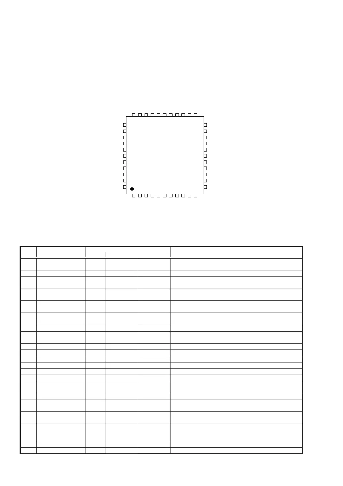
1. ICs
CSPFP44 Min UNIT U1
Terin Function
Pin Assinent Function
IO Port Denition
Function Description
IO Nor OFF
1 DCDET
I Low(0V) igh(3.3V)
DetectionsignalisforDCshortcircuit(3.3VVand12V).It
onlyworkinpower-onmode.
2 Port3.6PIO
- i- i-
Notuse
3 MCUSET1
I
igh(3.3V)
orLow(0V)
igh(3.3V)
orLow(0V)
MCUsettingpinbyeternailresistance.Defaultishigh
4 MCUSET2
I
igh(3.3V)
orLow(0V)
igh(3.3V)
orLow(0V)
MCUsettingpinbyeternailresistance.Defaultishigh
MCUPSON
O igh(3.3V) i-(0V)
Powerenableistocontrolthesystempoweronoff.ighisfor
thesystempoweronandlowisforstandbymode.
6 XOUT
O - -
XOUTCrystalOscillatorOutput
7 XIN
I - -
XINCrystalOscillatorInput
8 MCUSDA
IO igh(3.3V) igh(3.3V)
I2CDATAsignalisforEEPRMIC(24C02).
9 MCUCECIN
I igh(3.3V) igh(3.3V)
DMICECsignalinput.Itwakes-uptothesystemtopoweron
whenreceivetheCECpowercommandinstandbymode.
10 Port3.4PIO
- i- i-
Notuse
11 MCUSCL
O igh(3.3V) igh(3.3V)
I2CClocksignalisforEEPRMIC(24C02).
12 VSS
POWER - -
roundVoltage0V
13 RXVDD
POWER - -
VDDforRTC3.3V
14 RXIN
I - -
CrystalINforRTCoscillator
1 RXOUT
O - -
CrystalOUTforRTCoscillator
16 MCUSET3
I
igh(3.3V)
orLow(0V)
igh(3.3V)
orLow(0V)
MCUsettingpinbyeternailresistance.Defaultishigh
17 MCUAMUTE
O Low(0V) igh(3.3V) Mutingsignalforaudiooutput.ighisformutingandLowismutingoff.
18 DMIPOWERCTRL
O Low(0V) igh(3.3V)
PowerenableisfortheDMIVpowersupply.ighisfor
DMIworknormal.AndlowisforDMIoff.
19 VMUTE
O igh(3.3V) i-(0V)
MutingsignalforCVBSoutput.ighisforCVBSoutputis
enabled.AndlowdisabletheCVBSoutput.
20 CECRS232SWITC
O Low(0V) igh(3.3V)
SwitchsingalistoswitchMCUreceivethesingaloftheDMI
CECandRS232.ighisforMCUtoreceivethesignalofDMI
CECandlowisforswitchthosesingalinputtoMT830
21 MCUIICSCL
I igh(3.3V) i-(0V) I2CClocksignalthatcomunicatewithMT830.(Slavemode).
22 MCUIICSDA
IO igh(3.3V) i-(0V) I2CDatasignalthatcomunicatewithMT830.(Slavemode).
PGAVMID P3. SPICL
RXVDD
P2.4 T2EX CMPD
34
1
P1.4 SWC2
P1.5 SWC3
P3. CEX2 SWA1 CMPA
P3.1 CEX3 SWA2 CMPA
P3.4 SS
P1.2 SDA SWC
P2.5 T2 CMPC
PGAOUT1 P3.2 CEX4
PGAIN1 P3.3 CEX5
P4.2 SWB3
P2.2 TXD1
P2. CMPB
P2. CMPA SWA
RSTN
P1.1 ADD4 CEX1
P1. ADD3 CEX
P. RXD ADD2
P. TXD ADD1
P. PINT1. ADA1
P2.3 RXD1
P2.1 XOUT
P2. XIN
P1. T SWB PINT.1
P1. T1 SWB1 PINT.
P1.3 SCL SWC1
PGAOUT2 P3.5 MOSI
P4.3 SCL2
P
4.1 SDA2
VSS
PGAIN2 P3. MISO
P.5 PINT1.5 ADC2
P.4 PINT1.4 ADC1
P.3 PINT1.3 ADB2
P.1 PINT1.1 ADA2
P4. CEC
VDD
VDD25
P.2 PINT1.2 ADB1
RXIN
RXOUT
VSS
44
35
3
3
3
3
4
41
42
43
23
24
25
2
2
2
2
3
31
32
33
2
3
4
5
1
11
22
21
2
1
1
1
1
15
14
13
12
CSF
PFP44
 Loading...