CHAPTER 4. OPERATION 34
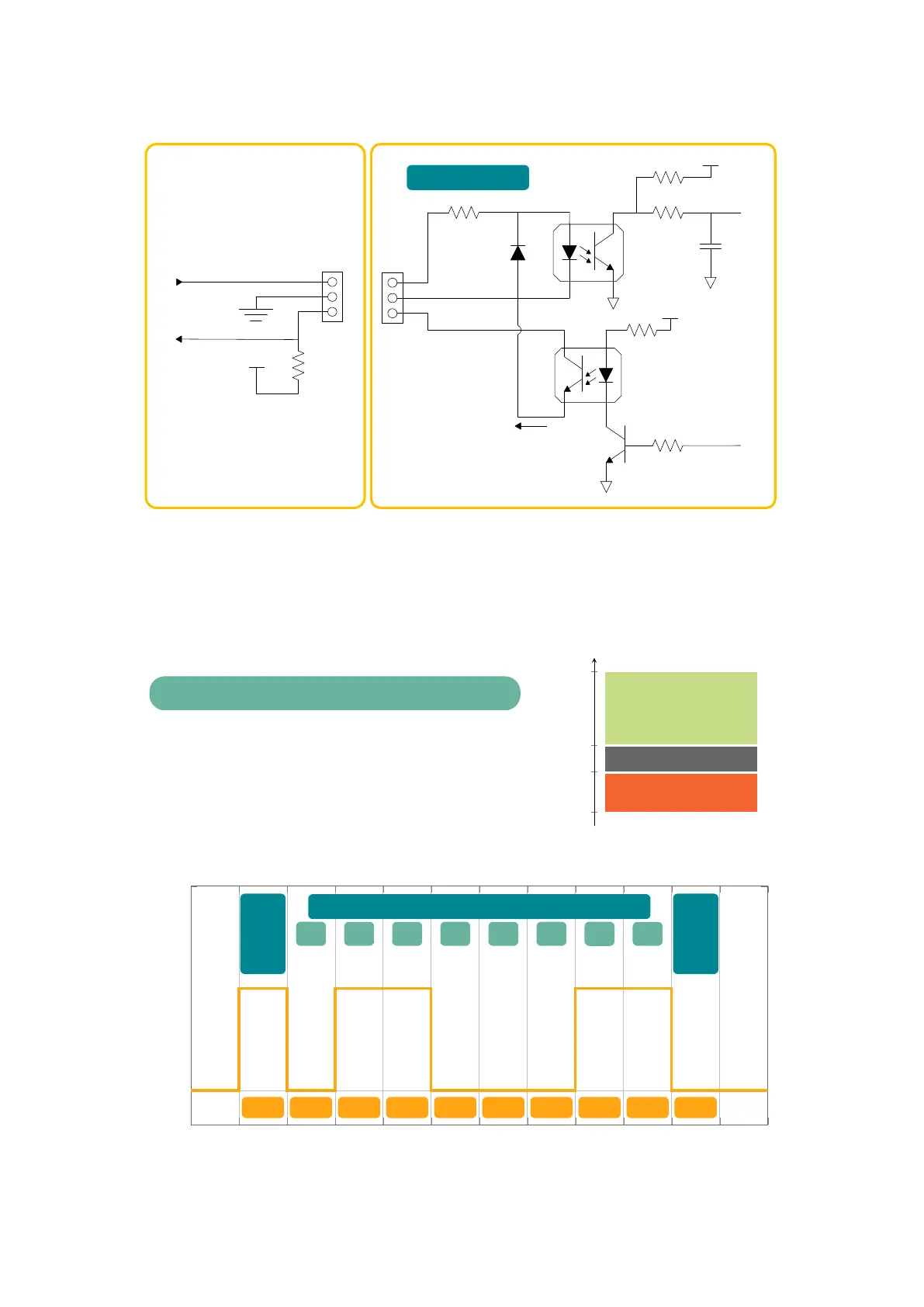
VCC
CN 203 pinout:
PIN 1 – Signal from Thermostat
PIN 2 – Thermostat GND
3
2
1
VCC
Inverter RX
Inverter TX
VCC
CN 204 pinout:
PIN 1 – Signal from Thermostat
PIN 2 – Thermostat GND
PIN 3 – Signal toThermostat
Collector current
range: 1 mA to 2 mA
CN 204
1
3
2
Thermostat TX
Thermostat RX
VCC
Thermostat TX
Inverter board
Figure 4.4: Electrical schematic of serial communication
To guarantee the correct functionality of serial communication, the signal to be sent
to the inverter must be according to the following values.
Signal specications
Voltage range -5 V to +15 V
TRUE state -5 V to +0.7 V
FALSE state +4.5 V to +15 V
Maximum current 2 mA @ 15 V
-5V
0.7V
4.5V
15V
TRUE state
Indenite state
FALSE state
↑
Start
bit
Data bits
Stop
bit
0
1 2
3
4
5
6 7
FALSE
TRUE
FALSE FALSE
TRUE TRUE TRUE
FALSE FALSE
TRUE
Time
Amplitude [V]
Example: 39h sent to inverter
The identication byte (1st byte), is used for command synchronization. Aſter in-
verter identies a valid A5h, it starts to read the next 4 bytes. Aſter reading, a re-