52 Appendix 2 Modbus Communication Protocol
EV3200 Door Control Inverter User Manual
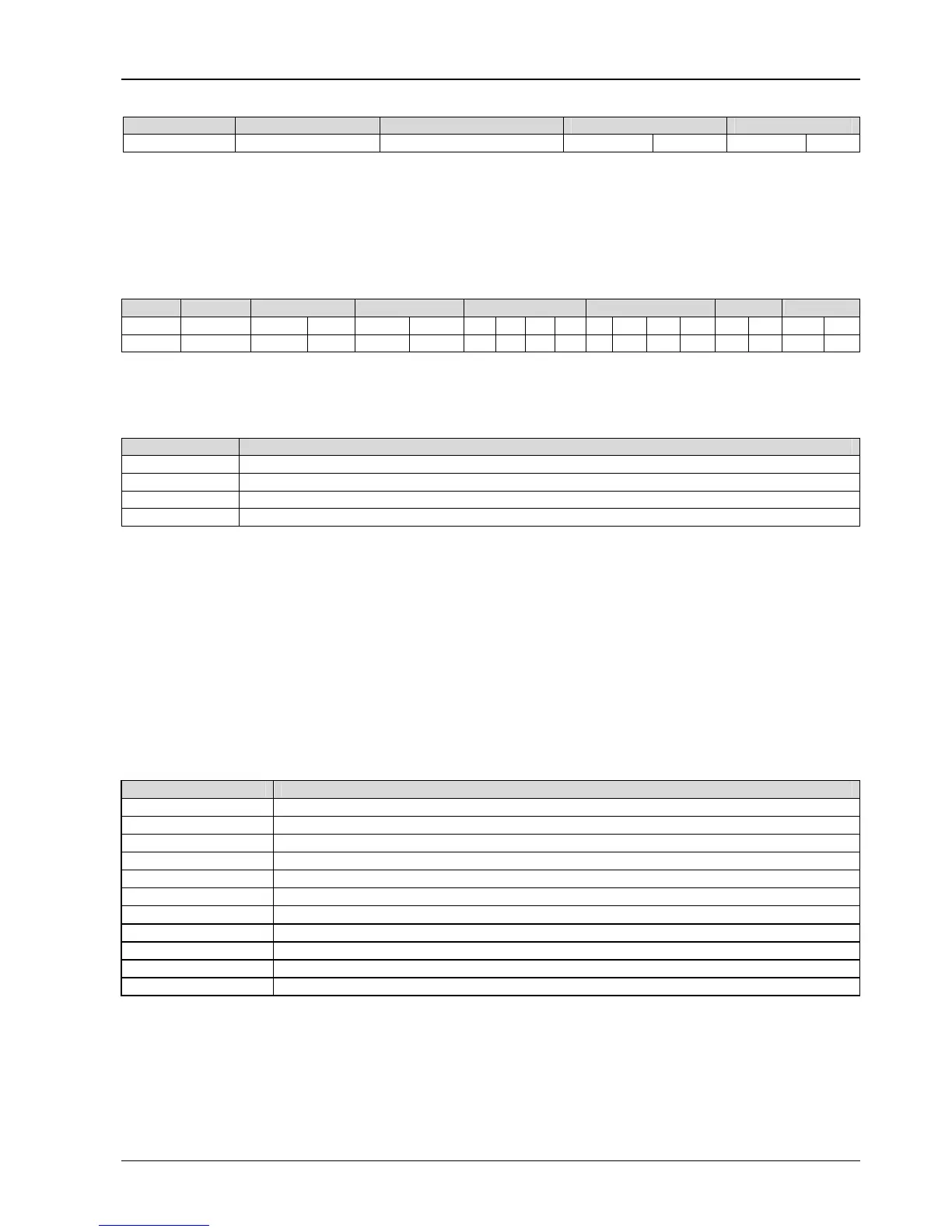
The table below shows the reply frame from Inverter No.1.
Address Function parameter Reply bytes Register content Check sum
0x01 0x03 0x02 0x00 0x00 0xB8 0x44
ASCII mode
In ASCII mode, the frame head is “0x3A”, and default frame tail is “0x0D” or “0x0A”. The frame tail can also be configured by
users. Except frame head and tail, other bytes will be sent as two ASCII characters, first sending higher nibble and then lower
nibble. The data have 7 bits. “A” ~ “F” corresponds to the ASCII code of respective capital letter. LRC check is used, the check
covers the information from slave address to data.
The following example shows the command frame of writing “1000 (0x3E8)” into Register 003 of Inverter No. 1.
Frame head Address Function parameter Register address Content written Check sum Frame tail
Code : 0 1 0 6 0 0 0 2 0 F A 0 4 8 CR LF
ASCII 3A 30 31 30 36 30 30 30 33 30 33 45 38 30 42 0D 0A
Protocol function
The main function of Modbus is to read and write parameters. Different function parameters decide different operation
requests. The Modbus protocol supports the following function codes:
Function parameter Description
0x03 Read inverter’s parameter and operation status parameters
0x06 Modify single inverter’s parameter or control parameters. Not save them upon power-off
0x41 Modify single inverter’s parameter or control parameters. Saving them upon power-off
0x10 Modify several inverters’ parameter or control parameters. Not save them upon power-off
All inverter’s parameters, control and status parameters are mapped to Modbus R/W Register. The R/W properties of the
parameters and their setting ranges are specified in the user manual. The group number of the inverter’s parameter maps to
the most significant byte of the register address, and the index number of the parameter in the group maps to the least
significant byte. The control and status parameters of the inverter are virtually taken as parameter group. The relationship of
group number of the parameters and the most significant byte of register address is listed below:
F0 group: 0x00. F1 group: 0x01. F2 group: 0x02.
F3 group: 0x03. F4 group: 0x04. F5 group: 0x05.
F6 group: 0x06. F7 group: 0x07. F8 group: 0x08.
F9 group: 0x09. FE group: 0x0E.
For example, the register address of F3.02: 0x302, register address of FE.01: 0xE01.
Inverter status parameter group: 0x33. Index of inverter status parameters:
Register address Parameter
0x3300 Operation status
0x3301 Running frequency
0x3302 Output current
0x3303 Output voltage
0x3304 Frequency setting
0x3305 DC bus voltage
0x3306 Software version
0x3307 Product configuration
0x3308 Angle of synchronous machine
0x3309 Reserved
0x3310 Input terminal group status (0: OFF 1: ON), X1 ~ X5, OD, CD corresponding to bits 0 ~ 6 respectively

 Loading...