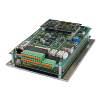
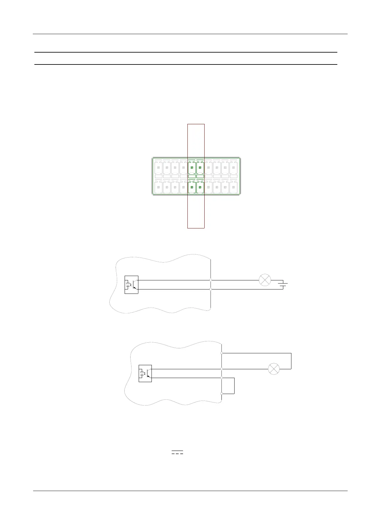
3.7 Optocoupler outputs (X2 / OUT1, OUT2)
The transistor connections, collector and emitter, of the optocoupler outputs are galvanically
isolated from the Reader electronics and are carried to the outside without any internal ancillary
circuitry on Terminal X2. The output must therefore be powered by an external power supply.
The digital outputs OUT1 and OUT2 can be used for the data clock interface. OUT1 => „Clock“,
OUT2 => „Data“
OUT1-E
IN1-
REL3-COM
REL2-COM
REL1-COM
GND
IN3-
IN2-
GND
OUT2-E
IN1+
OUT1-C
GND
IN3+
IN2+
OUT2-C
REL3-NO
REL2-NO
REL1-NO
24V
X2
Figure 10: Digital Output’s on terminal X2
Figure 11: Internal and possible external wiring of the digital output OUT1-2
Note:
The output is configured for max. 24 V / 30 mA.
Polarity reversal or overload on the output will destroy it.
The output is intended for switching resistive loads only.
 Loading...