Host Interface
4-8 C156-E205-01EN
4.3.1.5 Drive Address register
This register's bits are defined as shown below.
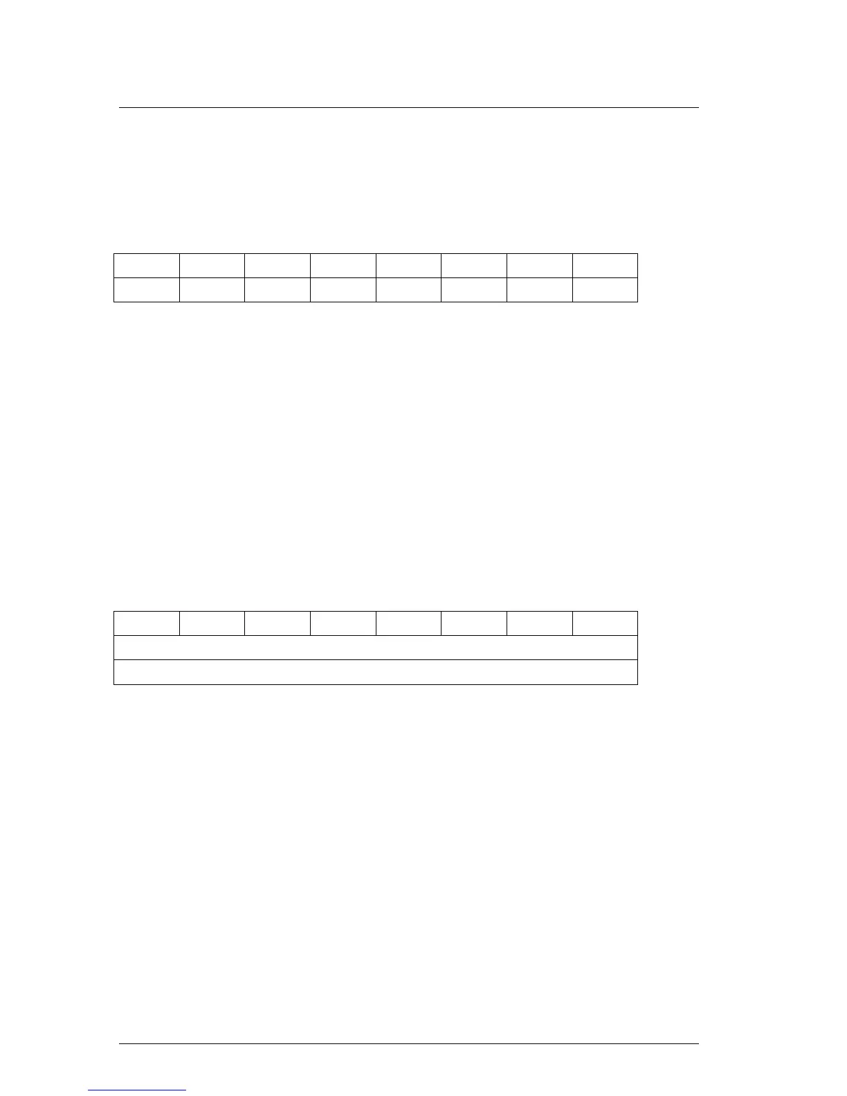
Table 4.6 Bit definitions of Drive Address register
76543210
HiZ nWTG nHS3 nHS2 NhS1 nHS0 nDS1 nDS0 Read
!
HiZ is always in the high-impedance state.
!
nWTG indicates the status of the ODD internal data write control signal
(Write Gate).
!
nHS3 indicates a binary complement of bits 3 to 0 of the drive select register.
!
nDS1 is the device select bit for device 1. It is 0 when device 1 is selected.
!
nDS0 is the device select bit for device 0. It is 0 when device 0 is selected.
4.3.1.6 ATAPI Byte Count register
This register's bits are defined as shown below.
Table 4.7 Bit definitions of ATAPI Byte Count register
76543210
Byte Count (Bits 7-0) R/W
Byte Count (Bits 15-8) R/W
!
This register is used for PIO transfer only. The ODD sets the byte count to be
transferred by the host in this register and sets DRQ to 1. The ODD does not
update this register until transfer starts.