English (GB)
17
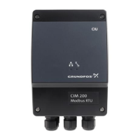
9.2 CIM configuration register block
Registers in this block can be read by means of function
codes 0x03 and/or 0x04. They can be written as holding
registers with function codes 0x06 and 0x10.
Address Register name Description
CIM
200
CIM
250
CIM
500
00001 SlaveMinimumReplyDelay
The minimum reply delay from the slave in ms.
Value range: 0-10000, i.e. up to 10 seconds reply delay. This delay is
typically used in conjunction with a radio modem. The delay value is
stored in the device and will remain after a power-off. The delay set here
will be added to the internal delay in the device.
Default value is 0.
● --
00002 RegisterOffset
An address offset that is added to all addresses above 00100.
Default value is 0.
Note: This offset does not affect the CIM configuration register block or
the CIM status register block addresses. The register offset value is
stored in the device and will remain after a power-off.
For most applications, this offset should not be changed.
●●●
00003 SoftwareDefinedModbusAddress
This register holds the active Modbus address. The default value is
0xE7 (231), and there is normally no need to change this value.
Note: For CIM 200, this value is used only when the transmission speed
is set to "Software-defined" on DIP switches SW4 and SW5.
Otherwise, it will be ignored by the slave.
●● -
00004 SoftwareDefinedBitRate
Modbus software-defined transmission speed enumeration.
The software-defined transmission speed value is stored in the device
and will remain after a power-off.
0: 1200 bits/s
1: 2400 bits/s
2: 4800 bits/s
3: 9600 bits/s
4: 19200 bits/s
5: 38400 bits/s.
Note: This value is used only when the transmission speed is set to
"Software-defined" on DIP switches SW4 and SW5 by selecting a value
outside the range [0; 247]. Otherwise, it will be ignored by the slave.
● --
00005 AutoAckControlBits
Used to select the behaviour of control bit acknowledgements from the
CIM/CIU.
0: Disabled.
Control bits are not automatically lowered when accepted by the device.
The user must lower the triggered control bit manually before the control
bit can be triggered again.
1: Enabled.
Control bits are automatically lowered when accepted by the device.
The user does not have to lower it manually [default].
●●●
00006 ReadWriteSeparation Not used. - - -
00007 ScadaCallBackRegister Not used. - - -
00008 NoDataActivityTimeout
The elapsed time with no data activity before the module issues a
"GPRS restart".
- ● -
00009 SoftwareDefinedParity
Parity setting to be used when using "software-defined" settings.
0: No parity [default]
1: Even parity
2: Odd parity.
Note: For CIM 200, this value is used only when the transmission speed
is set to "Software-defined" on DIP switches SW4 and SW5.
Otherwise, it will be ignored by the slave.
● --
00010 SoftwareDefinedStopBit
Stop bit setting to be used when using "software-defined" settings.
0: No stop bit
1: 1 stop bit [default]
2: 2 stop bits.
Note: For CIM 200, this value is used only when the transmission speed
is set to "Software-defined" on DIP switches SW4 and SW5.
Otherwise, it will be ignored by the slave.
● --
00011 ScadaPinCode
PIN code for SCADA systems, etc.
If GeneralStatus.ScadaPinCodeEnabled (register 00029, bit 0) is
enabled, the correct PIN code must be entered in this register in order to
gain access to remote control and configuration.
Verify acceptance in GeneralStatus.WriteAccess (register 00029, bit 1).
Programming of the SCADA PIN code takes place via the SMS
command SETSCADACODE. See "CIM 25X SMS commands"
(supplement to the installation and operating instructions) on the
CD-ROM supplied with the GSM module.
- ● -
 Loading...