PIN
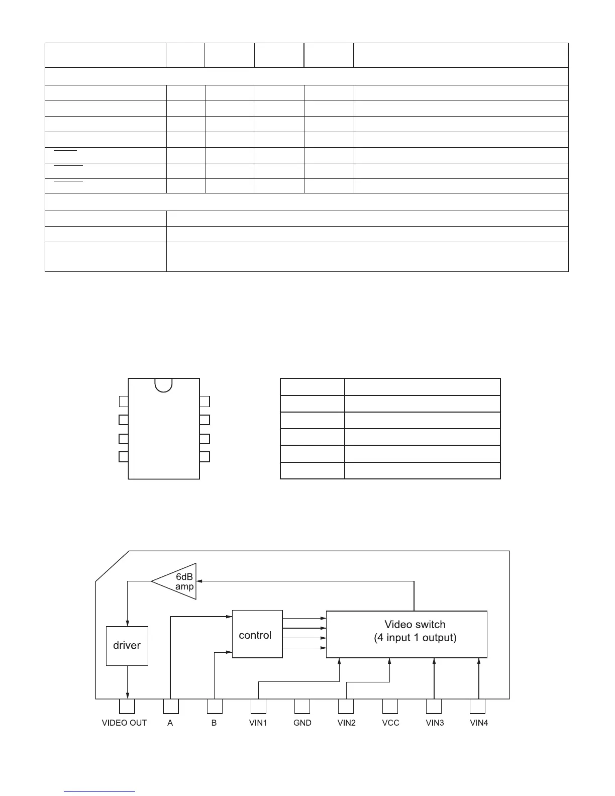
SIGNALNAME TYPE
(1)
PULL
(2)
GPIO
(3)
DESCRIPTION
NO.
Emulation/JTAG Port
TCK 35 I IPU N Test Clock
TMS 19 I IPU N Test Mode Select
TDI 28 I IPU N Test DataIn
TDO 29 OZ IPU N Test DataOut
TRST
21 I IPD N Test Reset
EMU[0]
32 IO IPU N EmulationPin 0
EMU[1]
34 IO IPU N EmulationPin 1
Power Pins
Core Supply(CV
DD
) 8, 16,20,33,44,53,57,65,77,85,90,101,123,128,132
IO Supply(DV
DD
) 10,31,42,50,60,68,73,81,92,103,112,125,136
Ground(V
SS
) 1,6, 13,15,18,26,30,36,40,47,54,62,69,72,78,82,87,95,99,106,109,114,118,124,129,
133,140
(1)
TYPE column refers to pin direction in functional mode. If a pin has more than one function with different directions, the functions
are
separated with a slash (/).
(2)
PULL column:
IPD = InternalPulldown resistor
IPU = InternalPullup resistor
(3)
If the GPIO column is 'Y', then in GPIO mode, the pin is configurable as an IO unless otherwise marked.

 Loading...