matching slave address or from the completion of a data byte transfer. When a slave address is
matched, the device must be placed in either the transmit mode and then write data to the HDR
register, or in the receive mode where it must implement a dummy read from the HDR register to
release the SCL line.
® SRW Bit
The SRW bit in the HSR register defines whether the microcontroller slave device wishes to read
data from the I
2
C bus or write data to the I
2
C bus. The microcontroller should examine this bit to
determine if it is to be a transmitter or a receiver. If the SRW bit is set to ²1² then this indicates that
the master wishes to read data from the I
2
C bus, therefore the microcontroller slave device must
be setup to send data to the I
2
C bus as a transmitter. If the SRW bit is ²0² then this indicates that
the master wishes to send data to the I
2
C bus, therefore the microcontroller slave device must be
setup to read data from the I
2
C bus as a receiver.
®
Acknowledge Bit
After the master has transmitted a calling address, any slave device on the I
2
C bus, whose own in
-
ternal address matches the calling address, must generate an acknowledge signal. This acknowl
-
edge signal will inform the master that a slave device has accepted its calling address. If no
acknowledge signal is received by the master then a STOP signal must be transmitted by the mas
-
ter to end the communication. When the HAAS bit is high, the addresses have matched and the
microcontroller slave device must check the SRW bit to determine if it is to be a transmitter or a re
-
ceiver. If the SRW bit is high, the microcontroller slave device should be setup to be a transmitter
so the HTX bit in the HCR register should be set to ²1², if the SRW bit is low then the
microcontroller slave device should be setup as a receiver and the HTX bit in the HCR register
should be set to ²0².
58
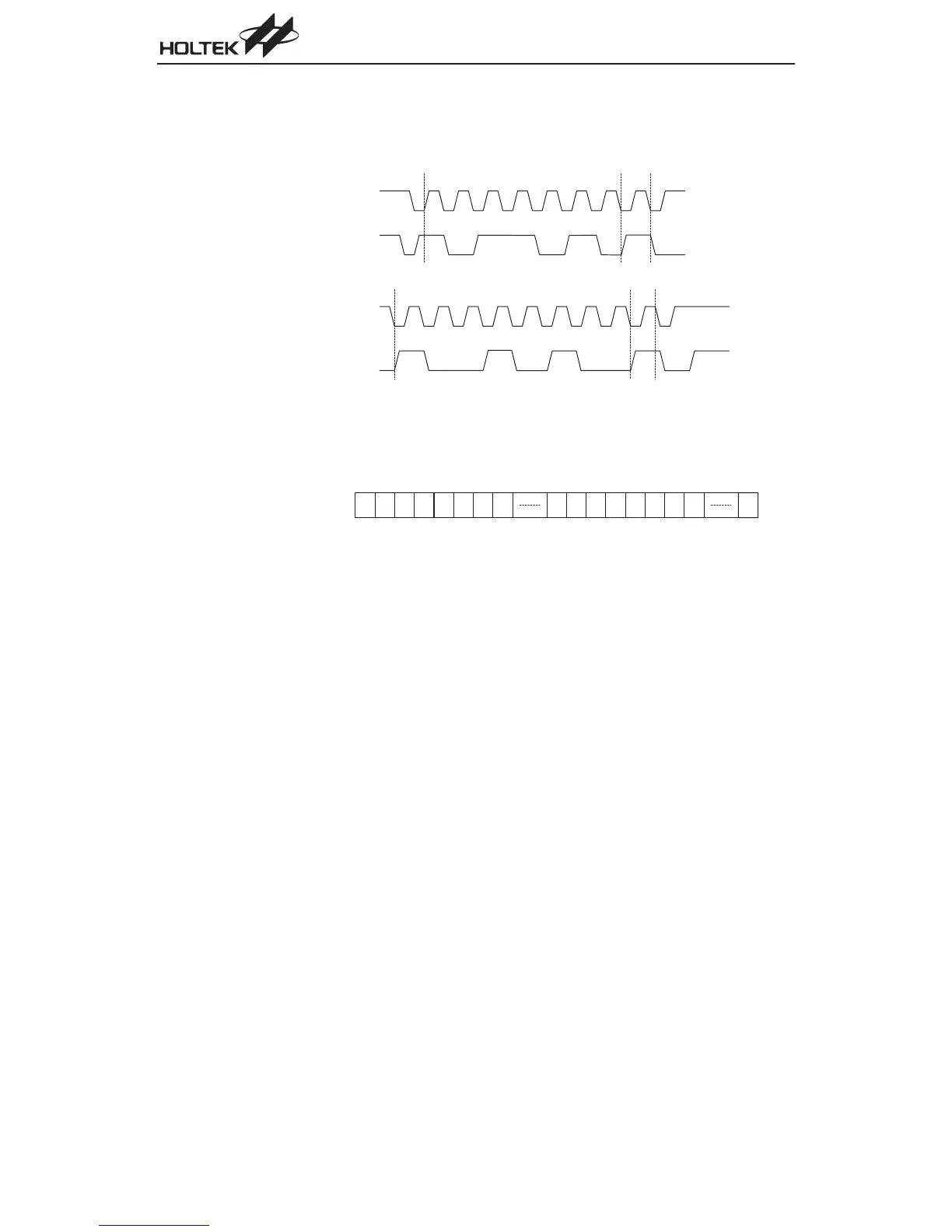
A/D Type MCU
D a t a
1 0 1 0 0 1 00
1
0
0 1 0 1 0
1
1
S = S t a r t ( 1 b i t )
S A = S l a v e A d d r e s s ( 7 b i t s )
S R = S R W b i t ( 1 b i t )
M = S l a v e d e v i c e s e n d a c k n o w l e d g e b i t ( 1 b i t )
D = D a t a ( 8 b i t s )
A = A C K ( R X A K b i t f o r t r a n s m i t t e r , T X A K b i t f o r r e c e i v e r 1 b i t )
P = S t o p ( 1 b i t )
S C L
S t a r t
S D A
S R W
A C K
A C K S t o p
S C L
S D A
S S A S R
M D A D A
S S A S R
M D A D A P
S l a v e A d d r e s s
I
2
C Communication Timing Diagram