Table 5-19 Mapping relationship between the pins in the input and output ports on the USLP2
Input Output
Label Pin Label Pin
IN0 IN0.1 OUT1 OUT1.1
IN0.2 OUT1.2
IN0.3 OUT1.4
IN0.4 OUT1.5
IN1 IN1.1 OUT1.3
IN1.2 OUT1.6
IN1.3 OUT1.7
IN1.4 OUT1.8
IN2 IN2.1 OUT0 OUT0.1
IN2.2 OUT0.2
IN2.3 OUT0.4
IN2.4 OUT0.5
IN3 IN3.1 OUT0.3
IN3.2 OUT0.6
IN3.3 OUT0.7
IN3.4 OUT0.8
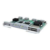
For details about the application of the USLP2, see 5.8.2 Configuration of the SLPU.
5 Auxiliary Devices of the BBU3900
BBU3900
Hardware Description
5-24 Huawei Proprietary and Confidential
Copyright © Huawei Technologies Co., Ltd.
Issue 11 (2010-11-10)
 Loading...