4 - 3
• PLL CIRCUITS
4-3 PLL CIRCUITS
4-3-1 GENERAL
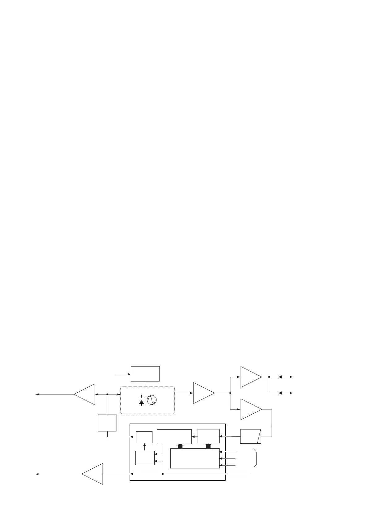
PLL circuits control the VCO circuit. IC19 is a PLL IC and
contains prescaler, programmable counter, programmable
divider, phase detector, charge pump in its package.
The VCO (Q76, D59, D60) directly generates both of the
transmit frequency and the 1st LO frequency. The VCO shift
circuit (Q77, D58) is used for switching the oscillating fre-
quencies between transmit and receive.
While receiving, only L44 is connected to the VCO and the
VCO generates the 1st LO frequency.
While transmitting, L44 and L45 are connected to the VCO
to generate the transmit frequency.
The PLL sets the divided ratio based on the N-data from the
CPU (IC8), and compares the phase of the VCO output with
the reference frequency (15.3 MHz) generated by X4.
If the oscillated signal drifts, the phase of its frequency
changes from the phase of the reference frequency, causing a
lock voltage change to compensate for the drift in the oscil-
lated frequency.
4-3-2 TRANSMIT LOOP
A portion of the generated signal at the VCO (Q76, D59, D60)
is applied to the PLL IC (IC19, pin 8) via buffer-amplifiers
(Q5, Q75). The applied signal is divided at the prescaler sec-
tion and programmable divider section, then applied to the
phase detector section.
The phase detector compares the input signal with the
reference frequency, and then outputs the control signal
(pulse-type) from pin 5 via the charge pump section. The
pulse-type signal is converted into DC voltage at the loop fil-
ter (R446–R448, C472–C474), and then applied to the VCO
(Q76, D59, D60) as the lock voltage.
4-3-3 RECEIVE LOOP
The generated 1st LO signal is applied to the PLL IC (IC19,
pin 8) via the buffer-amplifiers (Q5, Q75) and is divided at
the prescaler section and the programmable divider section,
then applied to the phase detector section.
The phase detector compares the input signal with the
reference frequency, and then outputs the control signal
(pulse-type) from pin 5. The pulse-type signal is converted
into DC voltage at the loop filter (R446–R448, C472–C474),
and then applied to the VCO (Q76, D59, D60) as the lock
voltage.
4-4 OTHER CIRCUITS
4-4-1 CTCSS/DTCS CIRCUIT (DECODING)
The CTCSS/DTCS signal from FM IF IC (IC2, pin 9) is fil-
tered at the LPF (Q53). The filtered signal is then applied to
the CPU (IC8, pin 5) to control the AF amplifier according to
the received CTCSS/DTCS signal.
4-4-2 CTCSS/DTCS CIRCUIT (ENCODING)
• CTCSS
The CTCSS signal is generated by the CPU (IC8) and output
from pin 139 and passed through the LPF (R224, C126, C129)
and CTCSS switch (Q38). The CTCSS signal is then applied
to the splatter filter (IC3, pin 13) to be mixed with the micro-
phone audio signals. The filtered CTCSS signal is then
output from pin 14 and applied to the digital/analog switch
(IC15, pins 8, 9 and pins 3, 4) via the analog switch (IC4;
pins 8, 9).
The CTCSS signal from the digital/analog switch (IC15, pin 3)
is applied to the D/A converter (IC10, pin 21) to adjust its
level. The level adjusted CTCSS signal is then applied to the
modulator circuit (D61).
• DTCS
The DTCS signal is also generated by the CPU (IC8) and
output from pin 139. The DTCS signal is applied to the
DTCS amplifier (IC23, pin 3) via DTCS switch (IC16, pins 1,
7). The amplified DTCS signal is applied to the D/A convert-
er (IC10, pin 13) to adjust its level. The level adjusted DTCS
signal is then applied to both of the modulator circuit (D61)
and the reference frequency oscillator (X4).
Loop
filter
R5
Buffer
Q75
Buffer
Q3
Buffer
Q74
Buffer
Q5
to transmitter circuit
to 1st mixer circuit
D3
D4
5
8
Q76, D59, D60
Q77, D58
VCO
IC1 MB15E03SL
×3
45.9 MHz 2nd LO
signal to the FM IF IC
(IC2, pin 2)
Q81
Shift register
Prescaler
Phase
detector
Charge
pump
Programmable
divider
PLLCK
PLLSTB
1
2
9
10
11
PLLDATA
"LOINV" signal
to the CPU (IC661, pin 34)
LPF
PLL control signals
from D/A converter (IC10, pins 6–8)
15.3 MHz reference signal
from reference frequency osciilator (X4)
VCO SHIFT