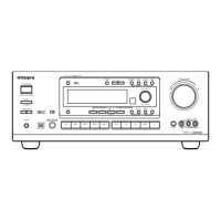
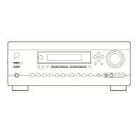
DTR-7.4
MAIN MICROPROCESSOR-TERMINAL DESCRIPTION
DTR-7.4
No. Function I/O Description
1 DSPDA O
Serial data output pin to transfer the data to DSP, DIR, Nettune DAC and Second PLL ICs.
2 DSPCL O Serial clock output pin to transfer the data to DSP, DIR and Nettune DAC ICs.
3 TNCL CLK Serial clock output pin for the tone control ICs.
4 Z2LMUT O Muting control signal output pin for line of zone 2 channel.
5 HPMUT O Muting control signal output pin for headphone.
6 Z2MUT O Muting control signal output pin for zone 2 channel when the power source is turned on.
7 AMUT O Muting control signal output pin of analog section.
8 VSS External data bus width select pin.
9 VSS Processor mode select pin
10 ~PRTCTTHM I Detection input pin for thermal protect.
11 SEC1H O Primary voltage select pin for main amplifier.
12 ~RESET System reset input pin
13 XOUT System clock output pin. Connect 16MHz ceramic resonator between #13 and #15.
14 VSS Ground pin.
15 XIN System clock input pin. Connect 16MHz ceramic resonator between #13 and #15.
16 VCC Power supply pin. Apply 5V.
17 I Not used.
18 PRTCTV I Detection input pin for protection circuit of abnormal voltage and current.
19 RDSCL I Serial clock input pin of RDS demodulator.
20 ~POFF I Power failure detection input pin.
21 ~RDSID I Identification input pin of RDS demodulator.
22 RDSDA I Serial data input pin to transfer RDS demodulator.
23 ~XPOR O Reset output pin to multi media microprocessor when power is turned on.
24 ~XDACS O Chip select output pin of DAC for Nettune.
25 ~XDARST O Reset signal output pin of DAC for Nettune.
26 ~TNCS1 O Chip select output pin for tone control IC of front channel.
27 NPOWER O Power supply control output pin of audio circuit.
28 TNDA O Serial data output pin to tone control IC.
29 IICSCL O
Serial clock output pin to Y/C, Component separation IC.
30 IICSDA O
Serial data output pin to Y/C, Component separation IC.
31 ~XPOWER O Power supply control output pin. Not used.
32 ~SUBRESET O Reset signal output pin for submicroprocessor.
33 ~SUBPOFF O Power off output pin to submicroprocessor
34 ~SUBREQ I Transfer request signal input pin for submicroprocessor.
35 MAINSO O Serial data output pin to transfer data between main and submicroprocessor.
36 MAINSI I Serial data input pin to transfer data between main and submicroprocessor.
37 MAINSCK O Serial clock output pin to transfer data between main and submicroprocessor.
38 ~MAINREQ O Request signal output pin to transfer data between main and submicroprocessor.
39 O
Not used.
40 (2ndBTACT) O
Not used.
41 I Mode setting pin to write the program on flash microprocessor.
42 ~DIRCS O Chip select output pin to DIR(AK4114) IC.
43 ~DIRRST O Reset output pin to DIR IC.
44 DFS O DFS output pin of DAC and CODEC ICs.
45 ~DAPD
P50
O Power down output pin of DAC.
46 I Write mode setting pin of flash microprocessor.
47 K I Lock input pin of second PLL IC.
48 2NDPLLCL O Clock output pin to second PLL IC.
49 2NDPLLCS O Chip select output pin of second PLL IC.
50 EX O Input select output pin of nettune.
No. Function I/O Description
51 ~CODECPD O Power down output pin of CODEC IC.
52 UPSMPL O Clock select output pin for up-sampling.
53 ~DSP1RST O Reset output pin of first DSP IC.
54 DSP1PM O PLL initializing output pin of first DSP IC.
55 DSP1GP8 O PCM or Non PCM information output pin of first DSP IC.
56 DSP1BST O Host I/F bootstrap output pin of first DSP IC.
57 ~DSP1HCS O Host I/F chip select output pin of first DSP IC.
58 ~DSP2RST O Second DSP reset output pin.
59 DSP2BST O Host I/F bootstrap output pin of second DSP IC.
60 ~DSP2HCS O Host I/F chip select output pin of second DSP IC.
61 (2ndBOOT) O
"L" fixed output pin.
62 VCC Power supply pin. Apply +5V.
63 (2ndPAGESE
O
"H" fixed output pin.
64 VSS Power supply pin. Ground
65 (HPAGE) O
"L" fixed output pin.
66 DTCDACCL O
Clock output pin for DAC of DTC.D
67 DTCDACCS O
Chip select output pin for DAC of DTC.D
68 DTCDACDA O
data output pin for DAC of DTC.D
69 (2ndGP10) O
"L" fixed output pin.
70 ~DSP2HACN I
Host I/F acknowledgement input pin of second DSP.2
71 ~DSP1HACN I
Host I/F acknowledgement input pin of first DSP.1.
72 DSP2HDOUT I
Host I/F serial data output pin to second DSP IC.
73 DIRINT1 I
INT 1 input pin of DIR IC.
74 DIRINT0 I
INT 0 input pin of DIR IC.
75 ~TNCS2 O Chip select output pin to tone control IC.
76 VPOWER O Power supply relay control output pin of video circuit.
77 12VTRGB O 12V trigger output pin B.
78 12VTRGA O 12V trigger output pin A.
79 12VTRGZ O 12V trigger output pin ZONE 2.
80 SPRLZ2 O Speaker relay control output pin for Zone 2.
81 SPRLF O Speaker relay control output pin for all channels.
82 APOWER O Power supply relay control output pin of audio circuit.
83 PLLCE O Chip enable output pin to PLL IC.
84 TUMUT O Muting control output pin for tuner section.
85 ~SD I Detection input pin for signal strength.
86 ~STEREO I Detection input pin for FM stereo broadcast.
87 AFSTB O Strobe signal output pin of analog function switch ICs.
88 AFDA O Serial data output pin for function switch ICs.
89 AFCL O Serial clock output pin for function switch ICs.
90 VPCL O Serial clock output pin for electric volume and PLL ICs.
91 VPDA O Serial data output pin for electric volume and PLL ICs.
92 VLSTB O Strobe output pin of electrical volume.
93 CDT0 I Serial data input pin for DSP and DIR ICs.
94 DSP1GP9 I Permission information input pin to read bit stream information of first DSP.
95 DSP1GP10 I INTREQ input pin of first DSP IC.
96 VSS Ground pin for A/D converter.
97 VOLH I Input pin to measure the output voltage of main amplifier.
98 VREF Reference voltage input pin for A/D converter.
99 VCC Power supply pin for A/D converter.
100 DSP1HDOUT I
Serial data output pin of host I/F of first DSP.
P57
P55

 Loading...