Contents
vii
4 Error Messages and Beep Codes
4.1 BIOS Error Messages ..................................................................................................77
4.2 Port 80h POST Codes .................................................................................................79
4.3 Bus Initialization Checkpoints ......................................................................................83
4.4 Speaker .......................................................................................................................84
4.5 BIOS Beep Codes........................................................................................................84
Figures
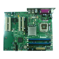
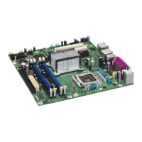
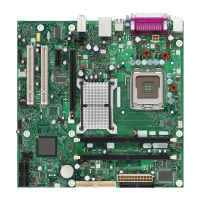
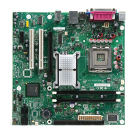
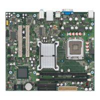
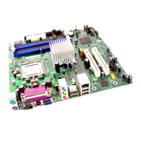
1. Board Components ......................................................................................................12
2. Block Diagram..............................................................................................................14
3. Memory Channel and DIMM Configuration..................................................................18
4. Dual Channel (Interleaved) Mode Configuration with Two DIMMs ..............................19
5. Dual Channel (Interleaved) Mode Configuration with Three DIMMs............................19
6. Dual Channel (Interleaved) Mode Configuration with Four DIMMs..............................20
7. Single Channel (Asymmetric) Mode Configuration with One DIMM.............................21
8. Single Channel (Asymmetric) Mode Configuration with Three DIMMs........................21
9. Front/Back Panel Audio Connector Options for High Definition Audio Subsystem......28
10. High Definition Audio Subsystem Block Diagram ........................................................28
11. LAN Connector LED Locations ....................................................................................29
12. Location of Thermal Sensors and Fan Connectors......................................................31
13. Location of the Standby Power Indicator LED .............................................................38
14. Detailed System Memory Address Map.......................................................................40
15. Back Panel Connectors................................................................................................47
16. Component-side Connectors .......................................................................................48
17. Connection Diagram for Front Panel Connector..........................................................53
18. Connection Diagram for Front Panel USB Connectors................................................54
19. Location of the Jumper Block.......................................................................................55
20. Board Dimensions........................................................................................................56
21. I/O Shield Dimensions..................................................................................................57
22. Processor Heatsink for Omni-directional Airflow..........................................................60
23. Localized High Temperature Zones.............................................................................61
Tables
1. Feature Summary ........................................................................................................10
2. Board Components Shown in Figure 1 ........................................................................13
3. Supported System Bus Frequency and Memory Speed Combinations .......................16
4. Supported Memory Configurations ..............................................................................17
5. LAN Connector LED States .........................................................................................30
6. Effects of Pressing the Power Switch ..........................................................................33
7. Power States and Targeted System Power .................................................................34
8. Wake-up Devices and Events......................................................................................35
9. System Memory Map ...................................................................................................41
10. DMA Channels.............................................................................................................41
11. I/O Map ........................................................................................................................42
12. PCI Configuration Space Map......................................................................................43
13. Interrupts......................................................................................................................44
14. PCI Interrupt Routing Map ...........................................................................................45