102 Datasheet
Signals Reference
All receiving agents observe the REQ[5:0]# signals to determine the transaction type and
participate in the transaction as necessary, as shown in Table A-10.
A.1.51 RESET# (I)
Asserting the RESET# signal resets all processors to known states and invalidates all caches
without writing back Modified (M state) lines. RESET# must remain asserted for one millisecond
for a “warm” reset; for a power-on reset, RESET# must stay asserted for at least one millisecond
after PWRGOOD and BCLKp have reached their proper specifications. On observing asserted
RESET#, all system bus agents must deassert their outputs within two clocks.
A number of bus signals are sampled at the asserted-to-deasserted transition of RESET# for the
power-on configuration.
Unless its outputs are tristated during power-on configuration, after asserted-to-deasserted
transition of RESET#, the processor begins program execution at the reset-vector
A.1.52 RP# (I/O)
The Request Parity (RP#) signal is driven by the requesting agent, and provides parity protection
for ADS# and REQ[5:0]#.
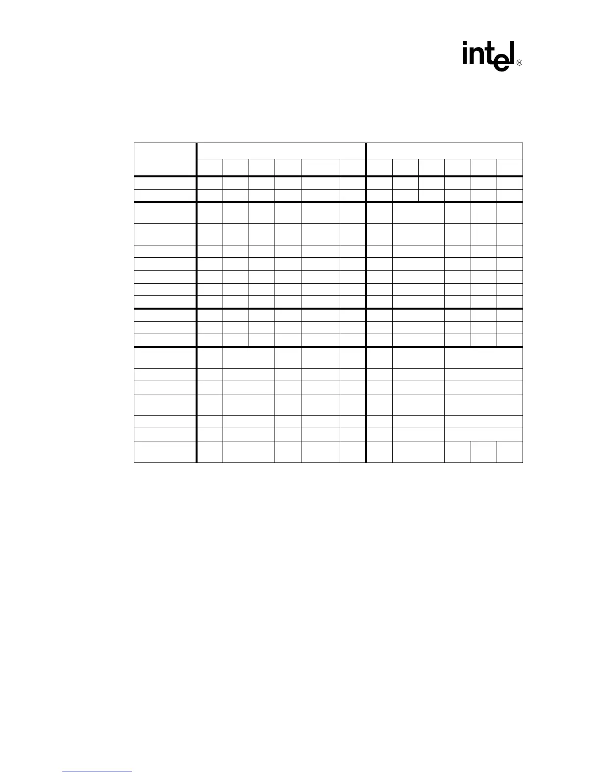
Table A-10. Transaction Types Defined by REQa#/REQb# Signals
Transaction
REQa[5:0]# REQb[5:0]#
5432 1 0543210
Deferred Reply0000 0 00xxxxx
Reserved
0000 0 10xxxxx
Interrupt
Acknowledge
0010 0 00DSZ[1:0]#000
Special
Transactions
0010 0 00DSZ[1:0]#001
Reserved 0010 0 00DSZ[1:0]#01x
Reserved 0010 0 10DSZ[1:0]#0xx
Interrupt 0010 0 10DSZ[1:0]#100
Purge TC 0010 0 10DSZ[1:0]#101
Reserved 0010 0 10DSZ[1:0]#11x
I/O Read 0100 0 00DSZ[1:0]#xxx
I/O Write 0100 0 10DSZ[1:0]#xxx
Reserved 0110 0 x0DSZ[1:0]#xxx
Memory Read &
Invalidate
0 ASZ[1:0]# 0 1 0 0 DSZ[1:0]# LEN[2:0]#
Reserved 0 ASZ[1:0]# 0 1 1 0 DSZ[1:0]# LEN[2:0]#
Memory Read 0 ASZ[1:0]# 1 D/C# 0 0 DSZ[1:0]# LEN[2:0]#
Memory Read
Current
1 ASZ[1:0]# 1 0 0 0 DSZ[1:0]# LEN[2:0]#
Reserved 1 ASZ[1:0]# 1 1 0 0 DSZ[1:0]# LEN[2:0]#
Memory Write 0 ASZ[1:0]# 1 WSNP# 1 0 DSZ[1:0]# LEN[2:0]#
Cache Line
Replacement
1 ASZ[1:0]# 1 WSNP# 1 0 DSZ[1:0]# 0 0 0