Datasheet 19
Electrical Specifications
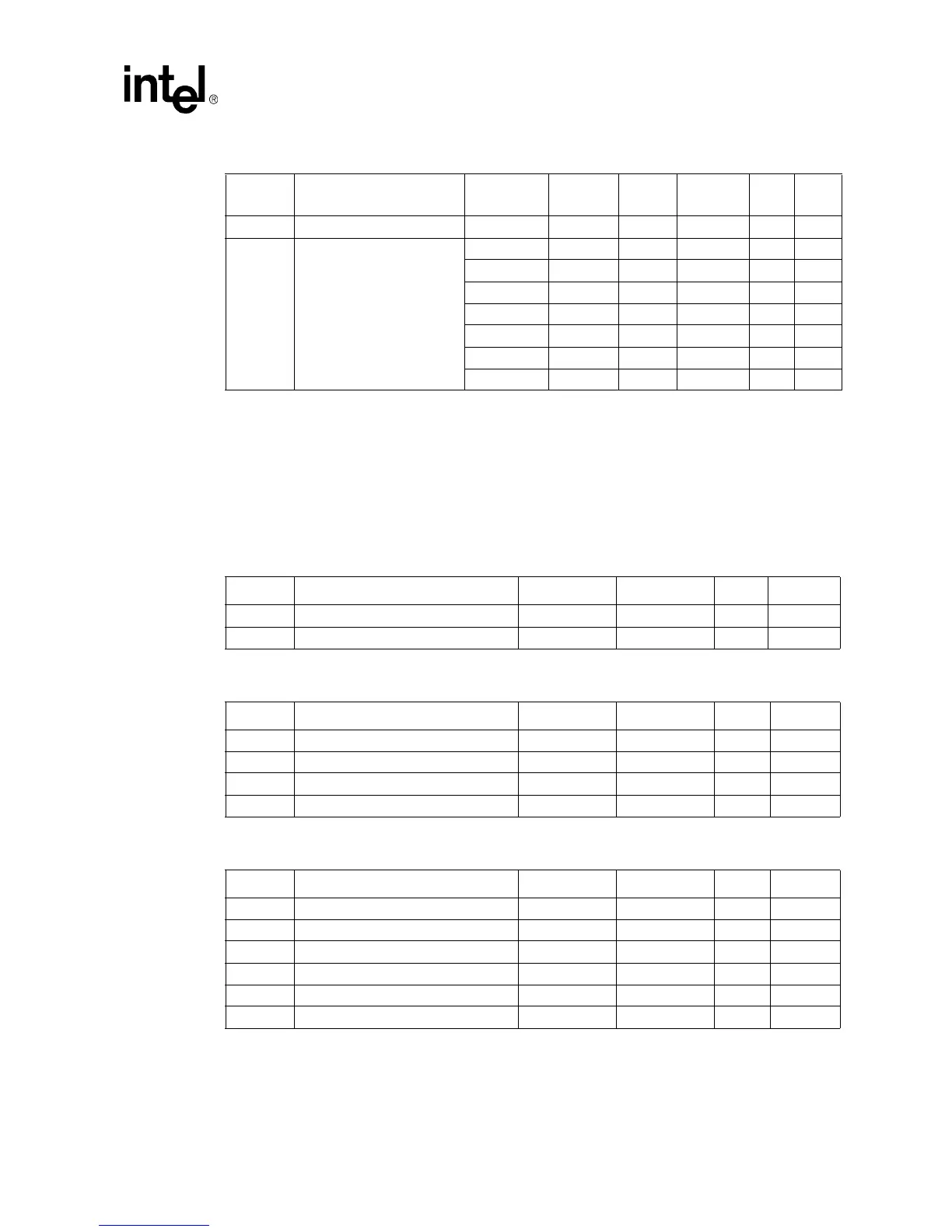
I
L
Leakage Current All ±100 µA
5
C
AGTL+
AGTL+ Pad Capacitance 900 MHz 3 pF
6
1.0 GHz 3 pF
6
1.3 GHz 1.5 pF
6
1.4 GHz 1.5 pF
6
1.5 GHz 1.5 pF
6
1.6 GHz 1.5 pF
6
1.66 GHz 1.5 pF
6
NOTES:
1. The typical transition point between V
IL
and V
IH
assuming 125 mV V
REF
uncertainty for ODT. V
REF_high
and V
REF_low
levels are
V
REF
±100 mV respectively, for a system bus agent using on-board termination. V
REF_high
and V
REF_low
levels are V
REF
±125
mV respectively, for a system bus agent using on-die termination.
2. Parameter measured into a 22.5 ohm resistor to 1.2V. Minimum V
OL
and I
OL
are guaranteed by design/characterization.
3. Calculated using off-die termination through two 45 ohm ±1% resistors in parallel.
4. Calculated using on-die termination to a 45 ±15% resistor measured at V
OL
.
5. At 1.2V ±1.5%. V
CTERM
, minimum ≤ Vpin ≤ V
CTERM
, maximum.
6. Total of I/O buffer with ESD structure and processor parasitics if applicable. Capacitance values guaranteed by design for all
AGTL+ buffers.
Table 2-5. Power Good Signal DC Specifications
Symbol Parameter Minimum Maximum Unit Notes
V
IL
Input Low Voltage 0.440 V
V
IH
Input High Voltage 0.875 V
Table 2-6. System Bus Clock Differential HSTL DC Specifications
Symbol Parameter Minimum Maximum Unit Notes
V
IH
Input High Voltage 0.78 1.3 V
V
IL
Input Low Voltage –0.3 0.5 V
V
X
Input Crossover Voltage 0.55 0.85 V
C
CLK
Input (Pad) Capacitance 1.75 pF
Table 2-7. TAP Connection DC Specifications
Symbol Parameter Minimum Maximum Unit Notes
V
IL
Input Low Voltage –0.3 0.5 V
1
NOTES:
1. There is a 100 mV hysteresis on TCK.
V
IH
Input High Voltage 1.1 1.57 V
1,
2
2. VIH, MAX = 1.5V + 5%, VOH, MAX = 1.2V +5%.
V
OL
Output Low Voltage 0.3 V
V
OH
Output High Voltage 1.2 V
2,
3
3. There is no internal pull-up. An external pull-up is always assumed. Max voltage tolerated at TDO is 1.5V.
I
OL
Output Low Current 20 mA
I
IC
Input Current 690 uA
4
4. Per input pin.
Table 2-4. AGTL+ Signals DC Specifications (Sheet 2 of 2)
Symbol Parameter
Core
Frequency
Minimum Typ Maximum Unit Notes