Rev. 1.3 29
C8051F340/1/2/3/4/5/6/7/8/9/A/B
4. Pinout and Package Definitions
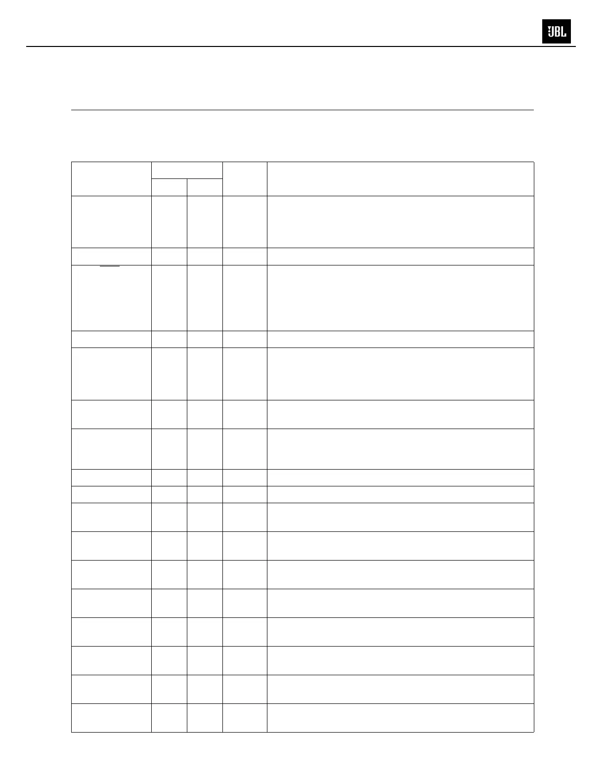
Table 4.1. Pin Definitions for the C8051F340/1/2/3/4/5/6/7/8/9/A/B
Name
Pin Numbers
Type Description
48-pin 32-pin
V
DD
10 6 Power In
Power
Out
2.7–3.6 V Power Supply Voltage Input.
3.3 V Voltage Regulator Output. See Section 8.
GND 7 3 Ground.
RST/
C2CK
13 9 D I/O
D I/O
Device Reset. Open-drain output of internal POR or V
DD
monitor. An external source can initiate a system reset by
driving this pin low for at least 15 µs. See Section 11.
Clock signal for the C2 Debug Interface.
C2D 14 — D I/O Bi-directional data signal for the C2 Debug Interface.
P3.0 /
C2D
— 10 D I/O
D I/O
Port 3.0. See Section 15 for a complete description of Port
3.
Bi-directional data signal for the C2 Debug Interface.
REGIN 11 7 Power In 5 V Regulator Input. This pin is the input to the on-chip volt-
age regulator.
VBUS 12 8 D In VBUS Sense Input. This pin should be connected to the
VBUS signal
of a
USB network. A 5 V signal on this pin indi-
cates a USB network connection.
D+ 8 4 D I/O USB D+.
D- 9 5 D I/O USB D–.
P0.0 6 2 D I/O or
A In
Port 0.0. See Section 15 for a complete description of Port
0.
P0.1 5 1 D I/O or
A In
Port 0.1.
P0.2 4 32 D I/O or
A In
Port 0.2.
P0.3 3 31 D I/O or
A In
Port 0.3.
P0.4 2 30 D I/O or
A In
Port 0.4.
P0.5 1 29 D I/O or
A In
Port 0.5.
P0.6 48 28 D I/O or
A In
Port 0.6.
P0.7 47 27 D I/O or
A In
Port 0.7.
MS-8