SCLS079E − MARCH 1984 − REVISED MARCH 2004
1
POST OFFICE BOX 655303 • DALLAS, TEXAS 75265
D
Wide Operating Voltage Range of 2 V to 6 V
D Outputs Can Drive Up To 10 LSTTL Loads
D Low Power Consumption, 20-µA Max I
CC
D Typical t
pd
= 7 ns
D ±4-mA Output Drive at 5 V
D Low Input Current of 1 µA Max
D Unbuffered Outputs
1
2
3
4
5
6
7
14
13
12
11
10
9
8
1A
1Y
2A
2Y
3A
3Y
GND
V
CC
6A
6Y
5A
5Y
4A
4Y
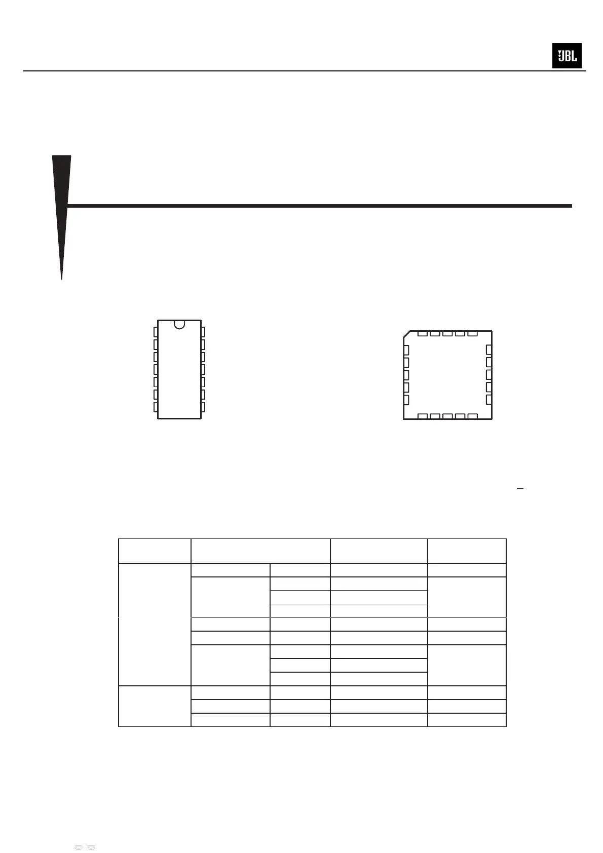
SN54HCU04 ...J OR W PACKAGE
SN74HCU04 . . . D, DB, N, NS, OR PW PACKAGE
(TOP VIEW)
3212019
910111213
4
5
6
7
8
18
17
16
15
14
6Y
NC
5A
NC
5Y
2A
NC
2Y
NC
3A
1Y
1A
NC
4Y
4A
V
6A
3Y
GND
NC
SN54HCU04 . . . FK PACKAGE
(TOP VIEW)
CC
NC − No internal connection
description/ordering information
The ’HCU04 devices contain six independent inverters. They perform the Boolean function Y = A
in positive
logic.
ORDERING INFORMATION
T
A
PACKAGE
†
ORDERABLE
PART NUMBER
TOP-SIDE
MARKING
PDIP − N Tube of 25 SN74HCU04N SN74HCU04N
Tube of 50 SN74HCU04D
SOIC − D
Reel of 2500 SN74HCU04DR
HCU04
†
Package drawings, standard packing quantities, thermal data, symbolization, and PCB design guidelines are
available at www.ti.com/sc/package.