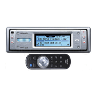
KD-LH3150, KD-LH3100
1-28 (No.49838)
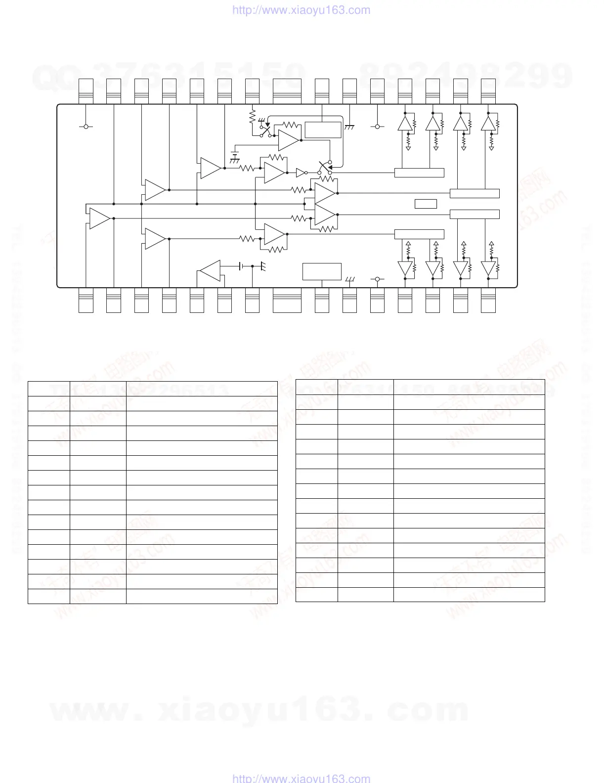
4.2 BA5830FP-X (IC681) : Power driver
• Pin layout & Block diagram
• Pin function
NOTE:
When PIN2,4,22,25 is high ("H"), the positive output pin of the driver is high ("H") and the negative output pin is low ("L").
When PIN23 is high ("H"), the positive output pin of CH4 is low ("L") and negative output pin is high ("H").
22232425262728 15161718192021
7654321 141312111098
T.S.D : thermal shutdown
Unit of resistance : [Ω]
-
+
-
+
-
+
-
+
-
+
-
+
-
+
BIAS
1.65V
2.4V
20k
10k
20k
Pre Vcc
-
+
20k
-
+
-
+
10k
10k
10k
10k
10k
10k
10k
10k
CH1
Level shifter
Pow
Vcc1
Pow
GND
PreGND
Level shifter
MUTE
CONTROL
Pow
Vcc2
Pow
GND
LD/SLED
CONTROL
-
+
10k
10k
-
+
10k
10k
CH2
CH4 CH3
Level shifter
-
+
Level shifter
T.S.D
-
+
10k
10k 10k 10k 10k
10k
10k 10k 10k 10k
-
+
-
+
-
+
-
+
H
H
L
L
Pin No. Symbol Function
1 OPIN2(-) CH2 Pre OP amplifier invert input
2 OPOUT2 CH2 Pre OP amplifier output
3 OPIN1(-) CH1 Pre OP amplifier invert input
4 OPOUT1 CH1 Pre OP amplifier output
5 REG-B Connect to external Tr Base
6 REG(+) Regulator terminal of output feedback
7 PreGND Pre Block and Regulator GND
8 MUTE Mute terminal
9 PowGND Power Block GND
10 PowVcc1 CH1, 2 Power Block Vcc
11 VO1(-) Driver CH1 negative output
12 VO1(+) Driver CH1 positive output
13 VO2(-) Driver CH2 negative output
14 VO2(+) Driver CH2 positive output
15 VO3(+) Driver CH3 positive output
16 VO3(-) Driver CH3 negative output
17 VO4(+) Driver CH4 positive output
18 VO4(-) Driver CH4 negative output
19 PowVcc2 CH3, 4 Power Block VCC
20 PowGND Power Block GND
21 CNT Control terminal
22 LDIN Loading input
23 OPOUTSL SLED Pre OP amplifier output
24 OPINSL(-) SLED Pre OP amplifier invert input
25 OPOUT3 CH3 Pre OP amplifier output
26 OPIN3(-) CH3 Pre OP amplifier invert input
27 BIAS BIAS input
28 PreVcc Pre-Block VCC
Pin No. Symbol Function
w
w
w
.
x
i
a
o
y
u
1
6
3
.
c
o
m
Q
Q
3
7
6
3
1
5
1
5
0
9
9
2
8
9
4
2
9
8
T
E
L
1
3
9
4
2
2
9
6
5
1
3
9
9
2
8
9
4
2
9
8
0
5
1
5
1
3
6
7
3
Q
Q
TEL 13942296513 QQ 376315150 892498299
TEL 13942296513 QQ 376315150 892498299
http://www.xiaoyu163.com
http://www.xiaoyu163.com
 Loading...