1-28 (No.22036)
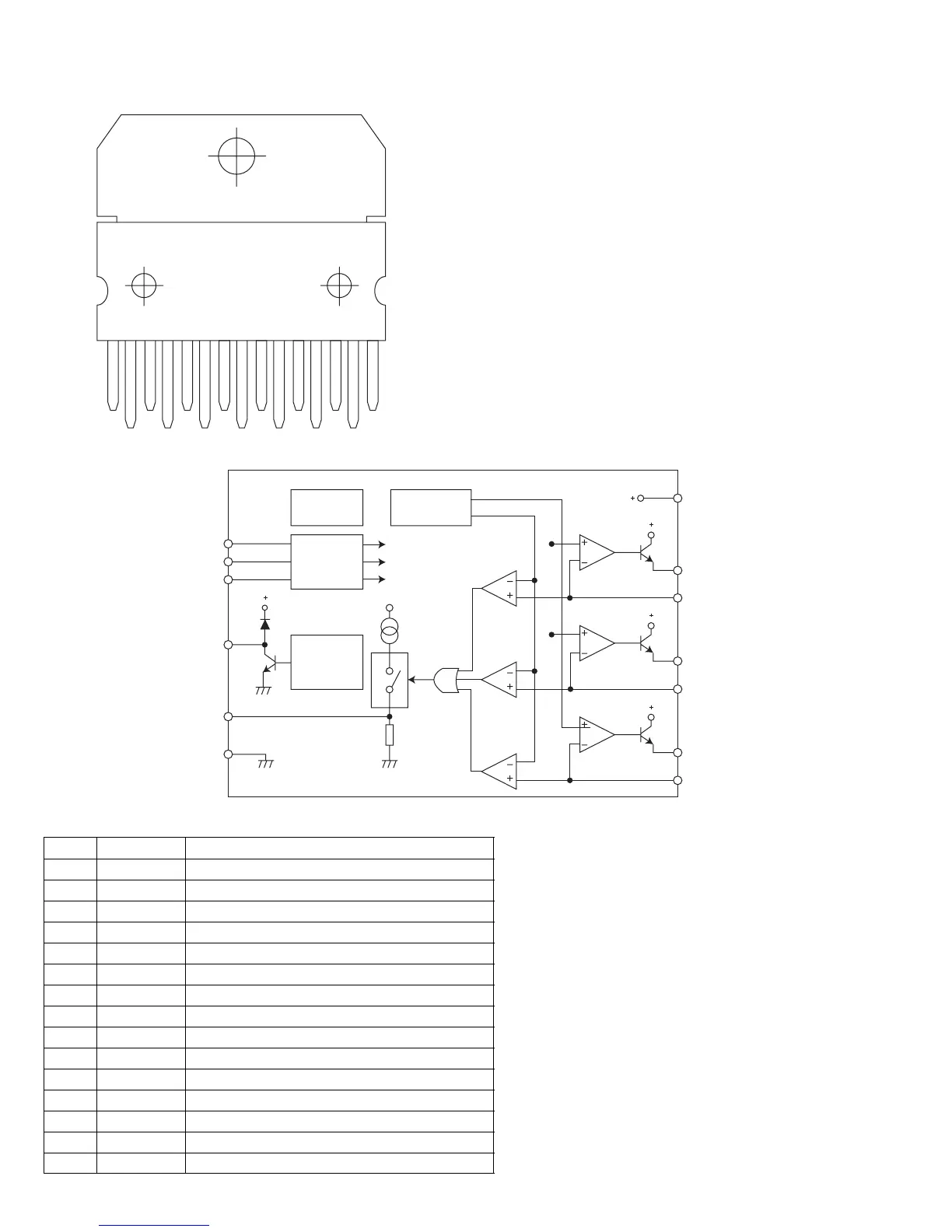
4.5 L4909 (IC910) : Regulator
• Pin layout
• Block diagram
• Pin functions
1234 56789101112131415
REG1
REG2
REG3
OVER
CURRENT
CHECK
ENABLE
CONTROL
THERMAL
SHUTDOWN
REFERENCE
GENERATOR
REG1
REG2
REG3
REF
REF+20%
6
7
9
5
4
8
11
10
14
15
1
2
3,13
VIN
VINB
VO1
FB1
VO2
FB2
VO3
FB3
GND
TRIG
OC
EN1
EN2
EN3
Pin No. Symbol Function
1 FB1 REG1 feedback voltage input
2 VO1 REG1 output voltage
3 VINA Input DC supply voltage
4 TRIG Trigger for external SCR (crowbar protection)
5 OC Over current warning output
6 EN1 REG1 enable input
7 EN2 REG2 enable input
8 GND Analog ground
9 EN3 REG3 enable input
10 FB3 REG3 feedback voltage input
11 VO3 REG3 output voltage
12 N.C. Not connected
13 VINB Input DC supply voltage
14 VO2 REG2 output voltage
15 FB2 REG2 feedback voltage input
 Loading...