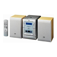
(No.22036)1-33
• Pin function
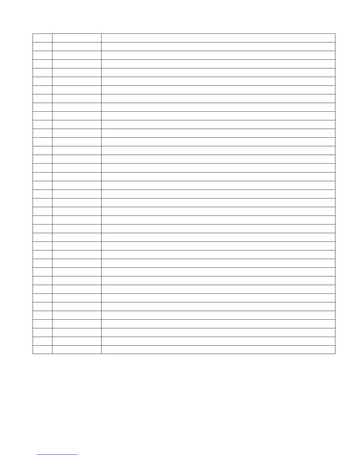
Pin No. Symbol Function
1 DI Serial data and clock input pin for control.
2 CE Chip enable pin.
3 VSS Ground pin.
4 LOPOUT Output pin of general-purpose operation amplifier.
5 LINM Non-inverted input pin of general-purpuse operation amplifier.
6 LINP Non-inverted input pin of general-purpuse operation amplifier.
7 LOUT ATT + equalizer output pin.
8 LSB Capacitor and resistor connection pin comprising filters for bass and super-bass band.
9 LBASS2 Capacitor and resistor connection pin comprising filters for bass and super-bass band.
10 LBASS1 Capacitor and resistor connection pin comprising filters for bass and super-bass band.
11 LTRE Capacitor and resistor connection pin comprising treble band filter.
12 LVRIN Volume input pin.
13 LSELO Input selector output pin.
14 L5 Input signal pin.
15 L4 Input signal pin.
16 L3 Input signal pin.
17 L2 Input signal pin.
18 L1 Input signal pin.
19 Vref 0.5 x VDD voltage generation block for analog ground.
20 R1 Input signal pin.
21 R2 Input signal pin.
22 R3 Input signal pin.
23 R4 Input signal pin.
24 R5 Input signal pin.
25 RSELO Input selector output pin.
26 RVRIN Volume input pin.
27 RTRE Capacitor connection pin comprising treble band filter.
28 RBASS1 Capacitor and resistor connection pin comprising filter for bass and super-bass band.
29 RBASS2 Capacitor and resistor connection pin comprising filter for bass and super-bass band.
30 RSB Capacitor and resistor connection pin comprising filter for bass and super-bass band.
31 ROUT ATT + equalizer output pin.
32 RINP Non inverted input pin of general-purpose operation amplifier.
33 RINM Non inverted input pin of general purpose operation amplifier.
34 ROPOUT Output pin of general-purpose operation amplifier.
35 VDD Supply pin.
36 CL Serial data and clock input pin for control.
 Loading...