DR600 Service Manual
0R 0R 0R
1
1 1 0 Ver6.0
NULL NULL NULL
0
0R 0R 0R
1
1 1 1 Ver7.0
NULL NULL NULL
0
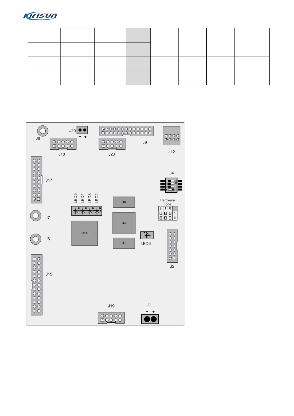
3.3.7 Baseband Board Interface and Indicator
Figure 3-16 Baseband Board Interface and Indicator
See Figure 3-16, The interfaces and indicators of banseband are as follows:
J1 is the 13.2V(+/-20%) DC input interface of the whole banseband mainboard, and the polarity should
be noted. The input circuit includes isolating magnetic inductor (L12) and chip insurance resistor (F1).
J2 is the JTAG adjustment interface of main processor, and it is used for program simulation adjustment.
J4 is the switch for boot mode. See“3.3.5Boot Mode” for details.
17

 Loading...