TM840 Service Manual
3.1.1 Transmitter Circuit
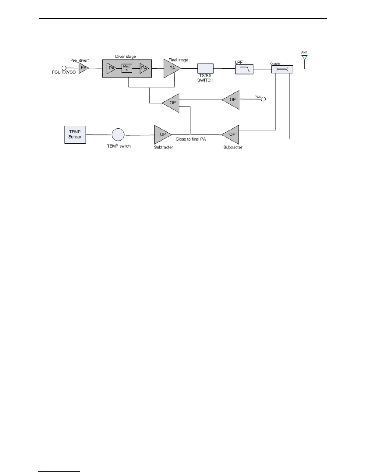
Figure 3-2 Transmitter Circuit Schematic
Transmitter circuit is composed of the following three parts:
RF Power Amplifier Circuit
The TX VCO generates a carrier signal, then it will be modulated and amplified before it goes into transmitter circuit. The
signal will pass through a Π type attenuator, and it is a process which allows the interstage isolation between the RF power
amplifier circuit and the TX VCO. The signal enters a pre-driver amplifier(U42) for the first amplification. Then the signal will
go to next driver amplifier(U51) to obtain further amplification, which will provide adequate power for the final stage amplifier
module(U100) to finish the final power amplification. After multi-stage amplification, the transmitter signal will pass through
the TX/RX switch, then enter the Low Pass Filter.
Low Pass Filter Circuit
The low pass filter is a high order low pass filter which can suppress harmonics. The filter is composed of lumped parameter
inductors and capacitors. Via this filter, the capability of attenuating, the spurious signal and harmonics can be increased
when the in-band ripple conditions are satisfied.
Auto Power Control Circuit( APC ,including the temperature detection and VSWR stationary wave detection
circuit )
When radio is transmitting, the power orientation coupler will detect forward and reverse output power, which will pass
through wave detecting diode for wave detecting and sampling. The sampled RF signal will pass through an attenuator, to
the PA power controller. The output voltage will be compared(IC1-A) firstly, the compared voltage will be compared again
with the pre-set voltage(IC3-A), the output voltage will be sent to PA power controller(IC2), then compared with the APC
reference voltage and sample signal for another comparison. The voltage will be output by the power controller and the
controller will adjust the grid voltage in the RF module to achieve VSWR stationary wave detecting and power control. In the
meantime, it will judge the VSWR base one the voltage and software pre-set conditions, and protect the power amplification
circuit by controlling the APC voltage. The APC voltage output by DAC will pass through a temperature-compensation circuit,
which allows compensating the power fluctuation that is caused by temperature difference. Then the temperature
protection circuit will amplify the voltage division network which is composed of thermistors, after an A/D conversion, it will be
4
 Loading...