TM840 Service Manual
provided to OMAP. OMAP will combine the VSWR rate to define the APC value to achieve the thermal protection.
3.1.2 Receiver Circuit
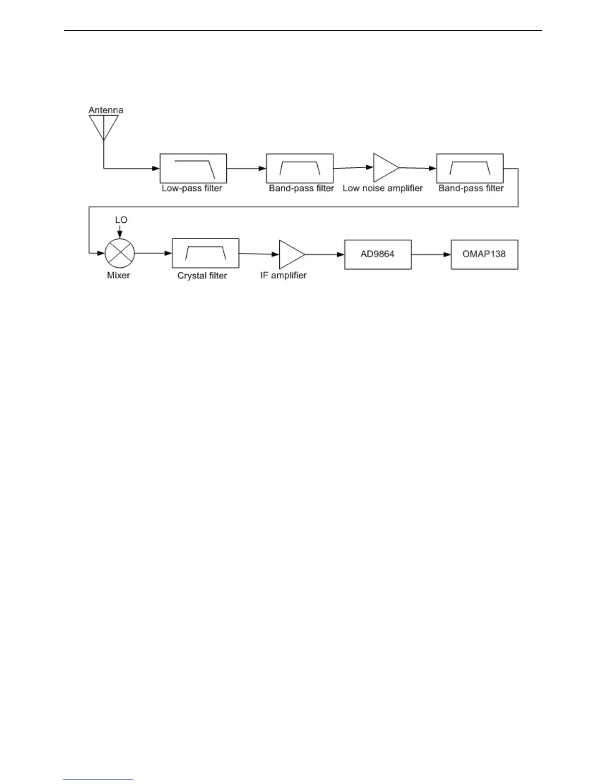
Figure 0-2 Receiver Circuit Schematic
The receiver circuit includes RF band pass filter, low-noise amplifier, mixer, IF filter, IF amplifier and IF processor.
The signal received from the antenna will pass the front end LPF and Tx-Rx switch controller, then it will enter the RF
electronic tuning band pass filter for frequency selecting. After that, it will be amplified by the low noise amplifier, then sent to
mix up with local oscillator signal which is provided by the first stage mixer IC3003 and VCO to achieve frequency conversion.
The first IF signal(UHF:73.35MHz,VHF:51.65MHz) output by the mixer will pass the IF filter to achieve channel selection.
Then it goes to Q18/19 for IF amplification, after that, the signal will be sent to AD9864 for second mix up and ADC sampling.
After the processing, the unmodulated I/Q digital signal will be output to DSP for FM/4FSK modulation, and after voice data
uncompressing, the signal will be sent into the audio codec chip for D/A conversion. Finally, the signal passes the audio
amplifier to speaker, then sent out.
The IF signal (UHF:73.35MHz,VHF:51.65MHz)output by IF amplifier will enter the AD9864 via pin 47 of U4000 for second
frequency mix up and ADC sampling, then output the unmodulated I/Q digital signal to DSP for FM/4FSK modulation.Please
refer to figure 3-4.
The reference frequency of AD9864 is 19.2MHz. The second local oscillator VCO is composed of external oscillator tube,
varactor and some other components. The local oscillator VCO provides a local oscillator signal(UHF:71.1MHZ,VHF:
49.4MHz). And the external LC syntony circuit generates a AD9864 clock frequency, which is 18MHz.
5
 Loading...