LTC2983
14
2983fc
For more information www.linear.com/LTC2983
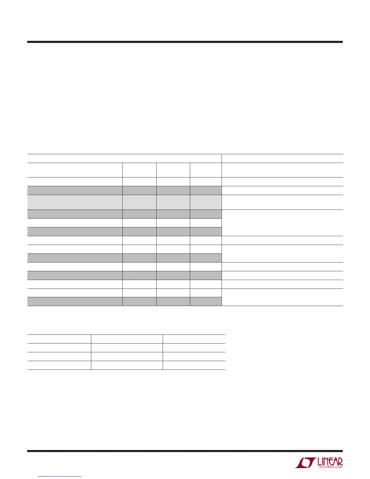
Table 2A. Memory Map
LTC2983 MEMORY MAP
SEGMENT START
ADDRESS
END
ADDRESS
SIZE
(BYTES)
DESCRIPTION
Command Status Register 0x000 0x000 1 See Table 6, Initiate Conversion, Sleep Command
Reserved 0x001 0x00F 15
Temperature Result Memory
20 Words - 80 Bytes
0x010 0x05F 80 See Tables 8 to 10, Read Result
Reserved 0x060 0x0EF 144
Global Configuration Register 0x0F0 0x0F0 1
Reserved 0x0F1 0x0F3 3
Measure Multiple Channels Bit Mask 0x0F4 0x0F7 4 See Tables 65, 66, Run Multiple Conversions
Reserved 0x0F8 0x0F8 1
Reserved 0x0F9 0x0FE 6
Mux Configuration Delay 0x0FF 0x0FF 1 See MUX Configuration Delay Section of Data Sheet
Reserved 0x100 0x1FF 256
Channel Assignment Data 0x200 0x24F 80 See Tables 3, 4, Channel Assignment
Custom Sensor Table Data 0x250 0x3CF 384
Reserved 0x3D0 0x3FF 48
OVERVIEW
Memory Map
The LTC2983 channel assignment, configuration, conver-
sion start, and results are all accessible via the RAM (see
Table 2A). Table 2B details the valid SPI instruction bytes
for accessing memory. The channel conversion results are
mapped into memory locations 0x010 to 0x05F and can be
read using the SPI interface as shown in Figure 1. A read is
initiated by sending the read instruction byte = 0x03
followed by the address and then data. Channel assign-
ment data resides in memory locations 0x200 to 0x24F
and can be programmed via the SPI interface as shown in
Figure 2. A write is initiated by sending the write instruc-
tion byte = 0x02 followed by the address and then data.
Conversions are initiated by writing the conversion control
byte (see Table 6) into memory location 0x000 (command
status register).
Table 2B. SPI Instruction Byte
INSTRUCTION SPI INSTRUCTION BYTE DESCRIPTION
Read 0b00000011 See Figure 1
Write 0b00000010 See Figure 2
No Opp 0bXXXXXX0X