LTC2983
58
2983fc
For more information www.linear.com/LTC2983
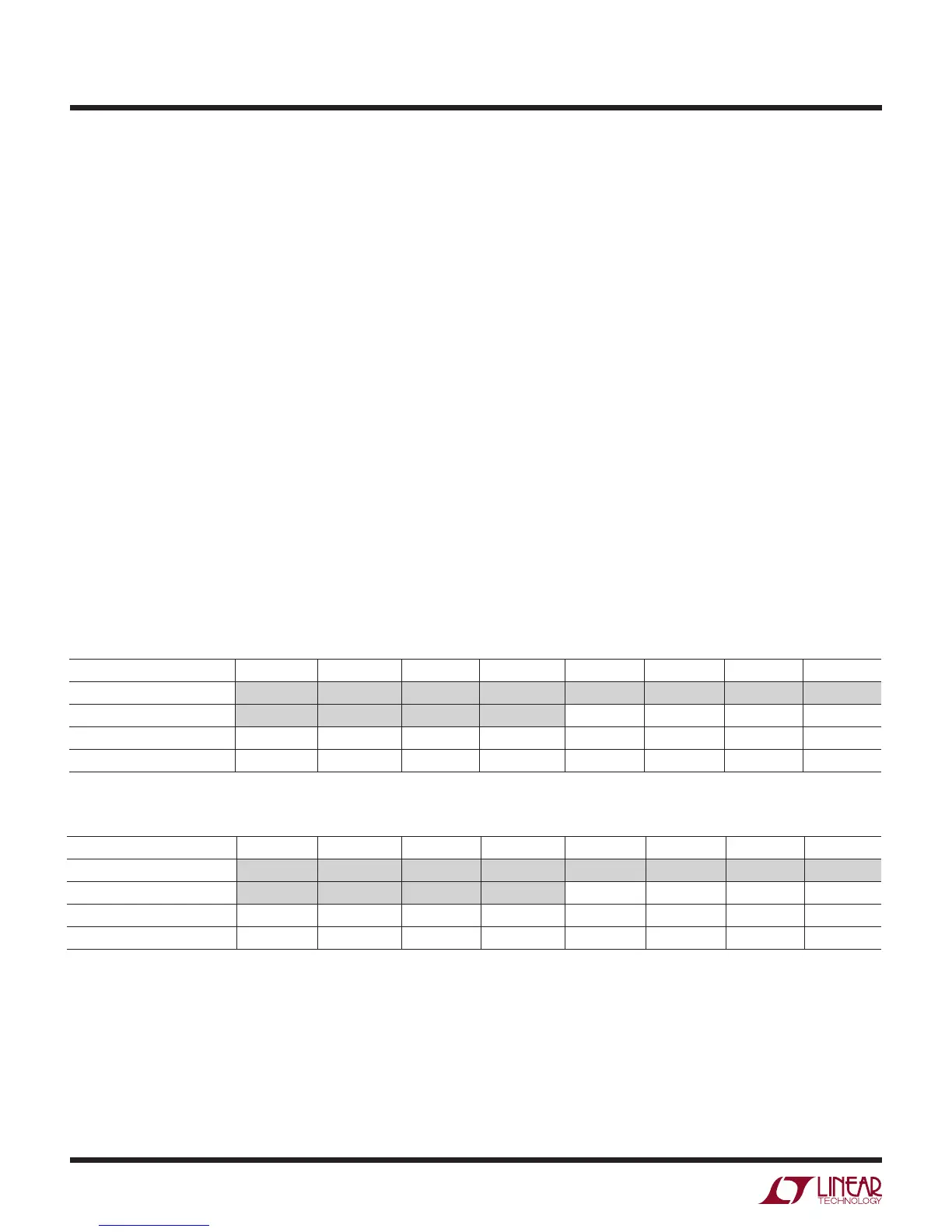
Table 65. Multiple Conversion Mask Register
MEMORY LOCATION B7 B6 B5 B4 B3 B2 B1 B0
0x0F4 Reserved
0x0F5 CH20 CH19 CH18 CH17
0x0F6 CH16 CH15 CH14 CH13 CH12 CH11 CH10 CH9
0x0F7 CH8 CH7 CH6 CH5 CH4 CH3 CH2 CH1
Table 66. Example Mask Register Select CH20, CH19, CH16, and CH1
MEMORY LOCATION B7 B6 B5 B4 B3 B2 B1 B0
0x0F4 Reserved
0x0F5 1 1 0 0
0x0F6 1 0 0 0 0 0 0 0
0x0F7 0 0 0 0 0 0 0 1
SUPPLEMENTAL INFORMATION
Running Conversions Consecutively on Multiple
Channels
Generally, during the Initiate Conversion state, a conver-
sion measurement is started on a single input chan-
nel determined by the channel number (bits B[4:0] =
00001 to 10100) written into memory location 0x000.
Multiple consecutive conversions can be initiated by writing
bits B[4:0]=00000 into memory location 0. Conversions
will be initiated on each channel selected in the mask
register (see Table 65).
For example, using the mask data shown in Table 66, after
1000000 is written into memory location 0, conversions
are initiated consecutively on CH20, CH19, CH16, and CH1.
Once the conversions begin, the INTERRUPT pin goes LOW
and remains LOW until all conversions are complete. If
the mask register is set for a channel that has no assign-
ment data, that conversion step is skipped. All the results
are stored in the conversion result memory locations and
can be read at the conclusion of the measurement cycle.
Entering/Exiting Sleep Mode
The LTC2983 can be placed into sleep mode by writing
0x97 to memory location 0x000. On the rising edge of
CS following the memory write (see Figure 2) the device
enters the low power sleep state. It remains in this state
until CS is brought low or RESET is asserted. Once one
of these two signals is asserted, the LTC2983 begins its
start-up cycle as described in State 1: Start-Up section
of this data sheet.
MUX Configuration Delay
The LTC2983 performs 2 or 3 internal conversion cycles
per temperature result. Each conversion cycle is performed
with different excitation and input multiplexer configura-
tions. Prior to each conversion, these excitation circuits
and input switch configurations are changed and an
internal
1ms (typical) delay ensures settling prior to the
conversion cycle in most cases.