LTC2983
5
2983fc
For more information www.linear.com/LTC2983
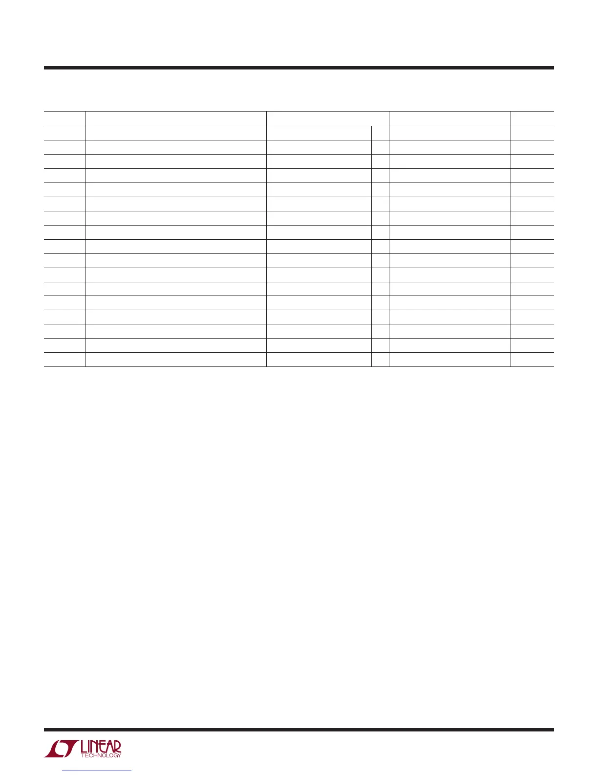
DIGITAL INPUTS AND DIGITAL OUTPUTS
SYMBOL PARAMETER CONDITIONS MIN TYP MAX UNITS
External SCK Frequency Range
l
0 2 MHz
External SCK LOW Period
l
250 ns
External SCK HIGH Period
l
250 ns
t
1
CS↓ to SDO Valid
l
0 200 ns
t
2
CS↑ to SDO Hi-Z
l
0 200 ns
t
3
CS↓ to SCK↑
l
100 ns
t
4
SCK↓ to SDO Valid
l
225 ns
t
5
SDO Hold After SCK↓
l
10 ns
t
6
SDI Setup Before SCK↑
l
100 ns
t
7
SDI HOLD After SCK↑
l
100 ns
High Level Input Voltage CS, SDI, SCK, RESET
l
V
DD
– 0.5 V
Low Level Input Voltage CS, SDI, SCK, RESET
l
0.5 V
Digital Input Current CS, SDI, SCK, RESET
l
–10 10 µA
Digital Input Capacitance CS, SDI, SCK, RESET 10 pF
LOW Level Output Voltage (SDO, INTERRUPT) I
O
= –800µA
l
0.4 V
High Level Output Voltage (SDO, INTERRUPT) I
O
= 1.6mA
l
V
DD
– 0.5 V
Hi-Z Output Leakage (SDO)
l
–10 10 µA
The l denotes the specifications which apply over the
full operating temperature range, otherwise specifications are at T
A
= 25°C.
Note 1: Stresses beyond those listed under Absolute Maximum Ratings
may cause permanent damage to the device. Exposure to any Absolute
Maximum Rating condition for extended periods may affect device
reliability and lifetime.
Note 2: All voltage values are with respect to GND.
Note 3: Full scale ADC error. Measurements do not include reference error.
Note 4: Guaranteed by design, not subject to test.
Note 5: The input referred noise includes the contribution of internal
calibration operations.
Note 6: MUX configuration delay = default 1ms
Note 7: Global configuration set to 60Hz rejection.
Note 8: Global configuration set to 50Hz rejection.
Note 9: Global configuration default 50Hz/60Hz rejection.
Note 10: The exact value of V
REF
is stored in the LTC2983 and used
for all measurement calculations. Temperature coefficient is measured
by dividing the maximum change in output voltage by the specified
temperature range.
Note 11:
Analog power-up. Command status register inaccessible during
this time.
Note 12:
Digital initialization. Begins at the conclusion of Analog Power-
Up. Command status register is 0 × 80 at the beginning of digital
initialization and 0 × 40 at the conclusion.
Note 13:
Long-term stability typically has a logarithmic characteristic
and therefore, changes after 1000 hours tend to be much smaller than
before that time. Total drift in the second thousand hours is normally less
than one third that of the first thousand hours with a continuing trend
toward reduced drift with time. Long-term stability will also be affected by
differential stresses between the IC and the board material created during
board assembly.
Note 14:
Hysteresis in output voltage is created by package stress
that differs depending on whether the IC was previously at a higher or
lower temperature. Output voltage is always measured at 25°C, but
the IC is cycled to the hot or cold temperature limit before successive
measurements. Hysteresis measures the maximum output change for the
averages of three hot or cold temperature cycles. For instruments that
are stored at well controlled temperatures (within 20 or 30 degrees of
operational temperature), it is usually not a dominant error source. Typical
hysteresis is the worst-case of 25°C to cold to 25°C or 25°C to hot to
25°C, preconditioned by one thermal cycle.
Note 15:
Differential Input Range is ±V
REF
/2.
Note 16:
RTD and thermistor measurements are made ratiometrically. As a
result current source excitation variation does not affect absolute accuracy.
Choose an excitation current such that largest sensor or R
SENSE
resistance
value, when driven by the nominal excitation current, will drop 1V or less.
The extended ADC input range will accommodate variation in excitation
current and the ratiometric calculation will negate the absolute value of the
excitation current.
Note 17: Do not apply voltage or current sources to these pins. They must
be connected to capacitive loads only, otherwise permanent damage may
occur.
Note 18: Input leakage measured with V
IN
= –10mV and V
IN
= 2.5V.