151
Table 2-2. Terminal Functions (continued)
PIN
SIGNAL NAME TYPE
(1)
PULL
(2)
GPIO
(3)
DESCRIPTION
NO.
Clocks
OSCIN 23 I - N 1.2-V Oscillator Input
OSCOUT 24 O - N 1.2-V Oscillator Output
OSCV
DD
25 PWR - N Oscillator 1.2-V V
DD
tap point (for filter only)
OSCV
SS
22 PWR - N Oscillator V
SS
tap point (for filter only)
CLKIN 17 I - N Alternate clock input (3.3-V LVCMOS Input)
PLLHV 27 PWR - N PLL 3.3-V Supply Input (requires external filter)
Device Reset
RESET 14 I - N Device reset pin
Emulation/JTAG Port
TCK 35 I IPU N Test Clock
TMS 19 I IPU N Test Mode Select
TDI 28 I IPU N Test Data In
TDO 29 OZ IPU N Test Data Out
TRST 21 I IPD N Test Reset
EMU[0] 32 IO IPU N Emulation Pin 0
EMU[1] 34 IO IPU N Emulation Pin 1
Power Pins
Core Supply (CV
DD
) 8, 16, 20, 33, 44, 53, 57, 65, 77, 85, 90, 101, 123, 128, 132
IO Supply (DV
DD
) 10, 31, 42, 50, 60, 68, 73, 81, 92, 103, 112, 125, 136
Ground (V
SS
) 1, 6, 13, 15, 18, 26, 30, 36, 40, 47, 54, 62, 69, 72, 78, 82, 87, 95, 99, 106, 109, 114, 118, 124, 129, 133, 140
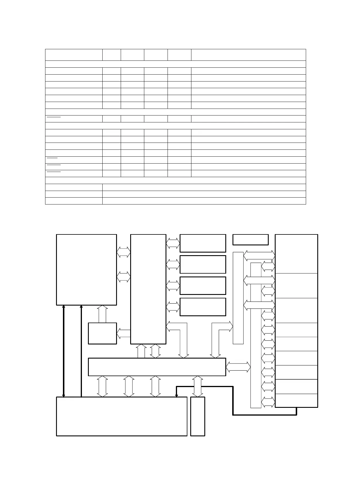
IC33 : TMS320DA708
2.15 Device Block Diagram
Program/Data
RAM
256K Bytes
256
256
Program/Data
ROM Page1
256K Bytes
256
256
256K Bytes
ROM Page3
Program/Data
Program/Data
ROM Page2
256K Bytes
3232
DMPPMP
CSP 32
256
Program
Cache
32K Bytes
64
D1
Data
R/W
R/W
Data
D2
64
256
Program
FetchINTI/O
C67x+ CPU
Memory
Controller
32
High-Performance
Crossbar Switch
32
McASP DMA Bus
JTAG EMU
32
32
32
32
32
32
32
Peripheral Configuration Bus
EMIF
32
Events
In
32
MAX1MAX0
32
CONTROL
32
Interrupts
Out
I/O
dMAX
McASP0
16 Serializers
McASP1
6 Serializers
McASP2
2 Serializers
DIT Only
SPI1
SPI0
I2C1
I2C0
RTI32
PLL
Peripheral Interrupt and DMA Events
32
32
32
32
Figure 2-3. DA708 DSP Block Diagram