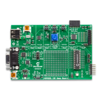
MCP2221 I
2
C Demonstration Board User’s Guide
DS50002480A-page 18 2016 Microchip Technology Inc.
2.4 TEST POINTS DESCRIPTION
Ta bl e 2- 2 describes the board’s test points.
J24 Jumper enabling the 4.7 pull-up resistors for the I
2
C data (SDA) and clock (SCL) lines on the board.
Consider removing it if the demonstration board connects to an external I
2
C slave circuit which already
has I
2
C pull-up resistors. The jumper is connected by default.
J25 I
2
C female connector; similar to the PICkit™ Serial Analyzer connector; however, this one only has the
power and I
2
C lines (V
DD
, GND, SDA, SCL). The white triangle indicates the first pin. Pins 1 and 6 are
not connected.
TABLE 2-1: MCP2221 BOARD JUMPERS CONFIGURATION (CONTINUED)
Jumper
Designator
Function Description
TABLE 2-2: MCP2221 BOARD TEST POINTS CONFIGURATION
Test Point
Designator
Description
TP1 Test point for measuring resistance or capacitance. If required, connect the positive pin of the polarized
capacitor to this test point.
TP2 Test point (connected to ground) for measuring resistance or capacitance. If required, connect the
negative pin of the polarized capacitor to this test point.
TP3 Test point for the ALERT
pin of the PAC1710. This test point is not used by the demonstration board’s
application.
TP4 Test point for the load side (target USB device) of the PAC1710 measuring circuit.
TP5 Test point for the source side (USB Host/PC) of the PAC1710 measuring circuit.
TP6 Test point for the I
2
C SDA line of the board.
TP7 Test point for the I
2
C SCL line of the board.
TP8 Test point connected to ground.