Chapter 2 DC Power Distribution
2.1 DC Regulation and Distribution
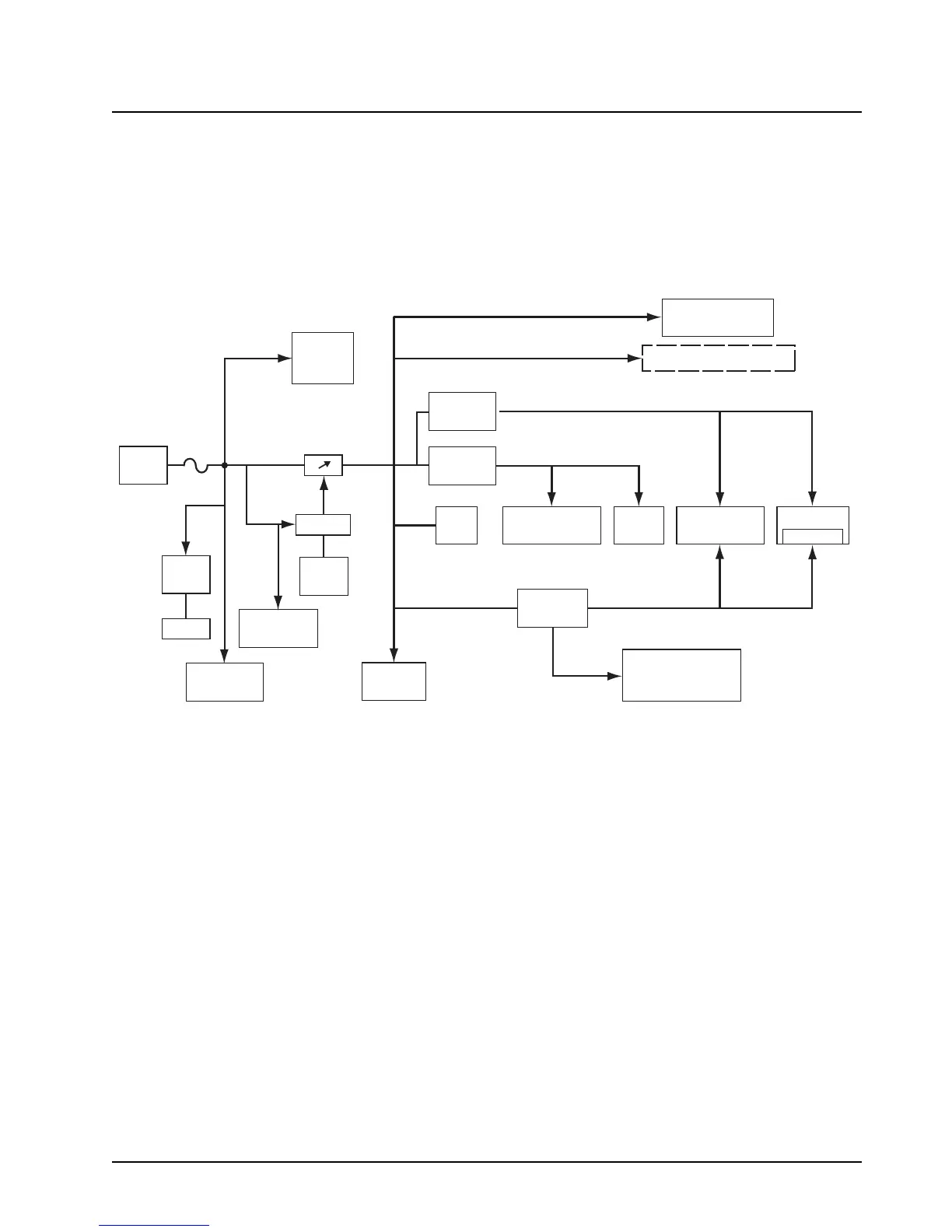
A block diagram of the DC power distribution throughout the radio is shown in Figure 2-1.
Figure 2-1. DC Power Distribution Block Diagram
Battery voltage enters at connector J301 and is routed through fuse F301 to become USWB+.
VR301 protects against ESD, and D301 provides reverse polarity protection. This voltage is routed
to:
• FET switch Q170 in the TX power control circuit (turned on during transmit)
• TX power amplifier module U110 (via R150)
• input pins of regulators U310, U320 and U330
• FET switch Q493 (turned on whenever the radio is on)
• on-off switch S444 (part of on-off-volume control) to become SWB+
SWB+
Fuse
Low Battery
Detect
Antenna
Switch
PA, Driver
PCIC(ALC)
LI Ion
3.3V
Reg.
Audio
Power
Amplifier
ASFIC_CMP
VCOBIC
FRACTN
LCD
Driver
5V
MECH.
SWB+
UNSWB+
Vdda
Accessories
20 pin Connector
Keypad/Option Board
Vddd
MCU, ROM
and EEPROM
Tx
Led
Control
7.5V
Battery
Vddd
Regulator
Vdda
Regulator
5V
Regulator
On/Off
Switch
RF AMP, IF AMP,
RX/TX Buffers
IFIC

 Loading...