HKLN4216A November 24, 2003
VHF Theory Of Operation: Keypad 4-7
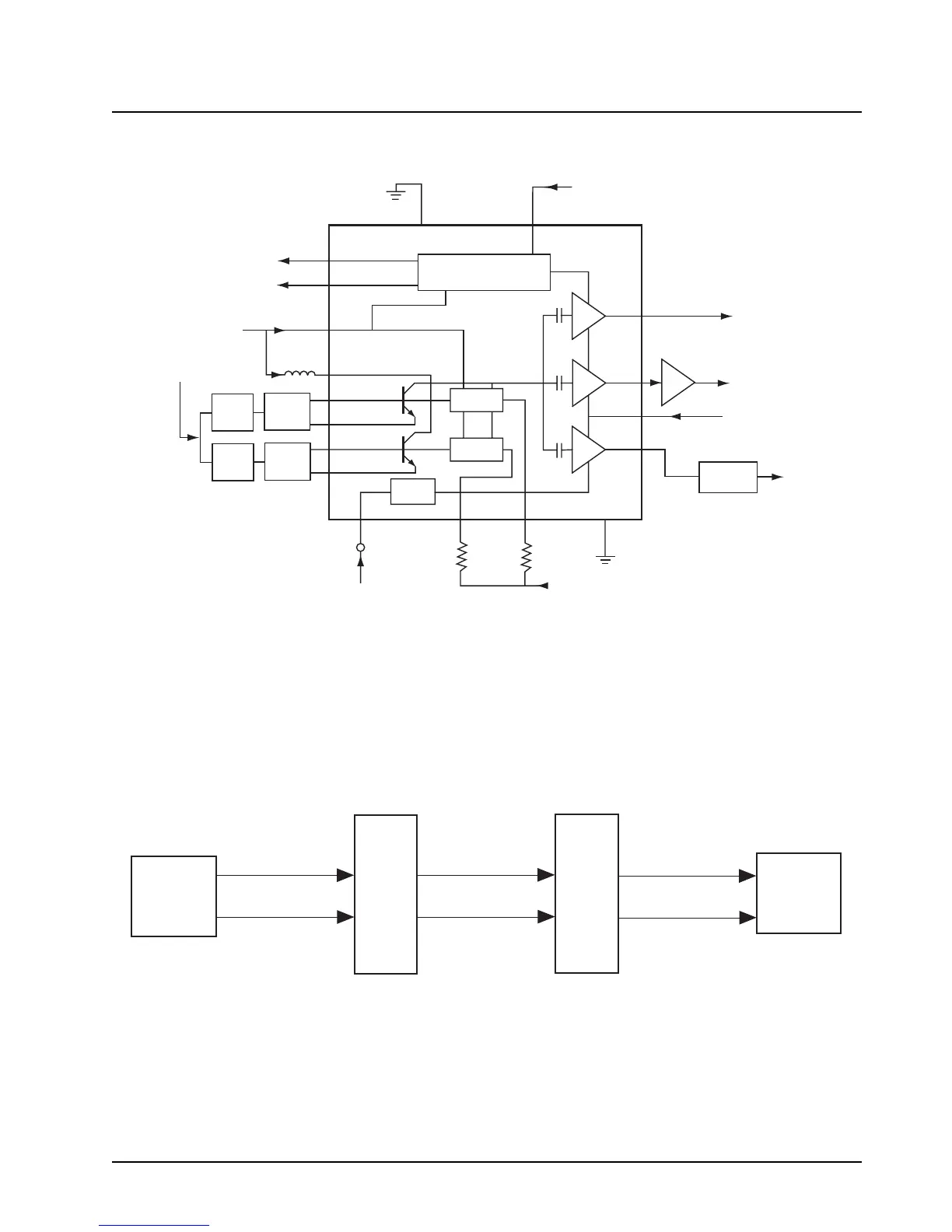
C267, and varactor D262. High-port audio modulation from the synthesizer IC is applied as
VCO_MOD to varactor D261 which modulates the transmit VCO.
Figure 4-5. VHF VCO Block Diagram
4.5 Keypad
The keypad block diagram is shown in Figure 4-6. Pressing a key creates two distinct voltages
KEYPAD_ROW and KEYPAD_COL. These voltages are sent directly to the radio’s microprocessor
on the main board. The microprocessor then interprets the voltage for KEYPAD_ROW and
KEYPAD_COL for each key press.
Figure 4-6. Keypad Block Diagram
Presc
RX
TX
Matching
Network
Pin 8
Pin 14
Pin 10
3V (U330 Pin 5)
VCC Buffers
U201 Pin 32
AUX3 (U201 Pin 2)
Prescaler Out
Pin 12
Pin 19
Pin 20
TX/RX/BS
Switching Network
U251
VCOBIC
Rx Active
Bias
Tx Active
Bias
Pin 2
Rx-I adjust
Pin 1
Tx-I adjust
Pins 9,11,17
Pin 18
Vsens
Circuit
Pin 15
Pin 16
TX VCO
Circuit
TX
Tank
RX VCO
Circuit
RX
Tank
Pin 7
Vcc-Superfilter
Collector/RF in
Pin 4
Pin 5
Pin 6
RX
TX
V_SF (U201 Pin 28)
NC
NC
Vcc-Logic
3V
(U330 Pin 5)
Steer Line
Voltage
(V_STEER)
Pin 13
Pin 3
TRB_IN
Buffer
Q280
RX INJ
V_SF
(U201 Pin 28)
TX INJ
Keypad
Button
MCP
Keypad Row
Keypad Row
Keypad Row
Keypad Column
Keypad Column
Keypad Column
28 Pin Connector
(keypad Board)
28 Pin Connector
(Main Board)

 Loading...