LIST OF ILLUSTRATIONS
Figure Page
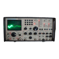
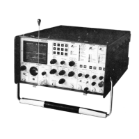
1-1 Communications System Analyzer ............................................................ 1-0
2-1 Accessories Supplied with
Analyzer ........................................................
2-4
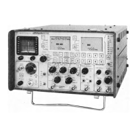
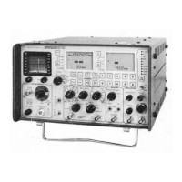
3-1 Typical Communication System Analyzer Packaging ........................................ 3-1
4-1 Controls, Indicators, and Connectors, Front Panel .......................................... 4-2
4-2 Controls, Indicators, and Connectors, Left Side
Panel
.......................................
4-3
4-3 Controls, Indicators, and Connectors, Rear Panel .......................................... 4-3
4-4 System Analyzer Time Base Calibrate Test Setup and CRT Display ......................... 4-13
4-5 Duplex Generation Test Setup and CRT Display .......................................... 4-14
4-6 Spectrum Test Setup and CRT Display .................................................... 4-16
4-7 Wattmeter Test Setup and CRT Display
....................................................
4-17
4-8 Test Setup for FM Receiver Sensitivity Using Generator and SINAD
Meter with CRT Display
...................................................................
4-18
4-9 Test Setup for Pager and Alert Functions with CRT Display
.................................
4-19
4-10 Test Setup for Using DVM and Signal Generate with CRT Display .......................... 4-20
5-1
Communication
System Analyzer, Top View Cover Removed
.................................
5-3
5-2 Communication System Analyzer, Bottom View Cover Removed ............................ 5-3
5-4 Generate Mode Block Diagram
............................................................
5-10
5-5 Power Meter Block Diagram
...............................................................
5-12
5-6
Monitor
Mode Block Diagram
............................................................
5-13
5-7 Duplex Generator Block Diagram
..........................................................
5-15
5-8
Code Synthesizer Block Diagram
.........................................................
5-16
5-9
Frequency Counter Block Diagram
.......................................................
5-17
5-10
Digital
Voltmeter (DVM) Block Diagram
....................................................
5-18
5-11 Oscilloscope Block Diagram ............................................................ 5-20
5-12 Sinad Meter Block Diagram
.............................................................
5-22
5-13 Scope Amplifier
Alignment
Points
.........................................................
5-23
5-14 Front Panel Interface
Alignment
Points
....................................................
5-26
5-15
Scope/DVM Control
Alignment
Points
.....................................................
5-27
5-16
Horizontal
Time
Base
Alignment Points
....................................................
5-27
5-17 DVM Input
Buffer
Alignment
Points .......................................................
5-28
5-18 Scope/DVM
Control
Test Point
Numbering .................................................
5-28
5-19 Processor
I/O
A/D
Alignment
Points
.......................................................
5-29
—-5-20 Scope/DVM
Control
Char Sweep
and
Sinad Alignment
Points ..............................
5-30
VI
 Loading...