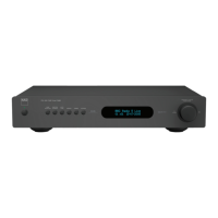
Pin Description
The status of the following GPIO pins are latched at the rising edge of nRESET and used to determine the system bus width and
boot mode. External devices must not drive output levels onto these pins during reset period.
Pin Name State during reset State after reset During normal function with DAI enabled
GPIO_A[9] / BW[1]
GPIO_A[8] / BW[0]
Bus Width Configuration Input Normal GPIO Input Mode GPIO Output Mode for 2-Wire Interface Clock and Data
GPIO_B[24] / BM[2]
GPIO_B[22] / BM[1]
GPIO_B[21] / BM[0]
Boot Mode Configuration Input Normal GPIO Input Mode
DAO (I2S Digital Audio Output)
LRCK (I2S Word Clock Output)
BCLK (I2S Bit Clock Output)
Refer to sections “BOOTING PROCEDURE” and “MEMORY CONTROLLER” for detailed description of BW[1:0] and BM[2:0].
In case of the TCC763, TCC764 and TCC766, GPIO_B[22:21]/BM[1:0] signals are connected to internal audio
CODEC pins which have on-chip pull-down resistor. If external pull-up resistors are required for these pins,
4.7k: is recommended.
The TCC76x is a CMOS device. Floating level on input signals cause unstable device operation and abnormal
current consumption. Pull-up or pull-down resistors should be used appropriately for input or bidirectional pins.
Notation
I : Input
O: Output
I/O: Bidirectional
AI: Analog Input
AO: Analog Output
PWR: Power
GND: Ground
TCC760 Pin Description
Table 1.2 TCC760 Pin Description
Signal Name Shared Signal Pin # Type Description – TCC760
External Memory Interface Pins
SD_CKE GPIO_B[0] 56 I/O SDRAM Clock Enable signal. Active high. / GPIO_B[0]
SD_CLK GPO 44 I/O
SDRAM Clock / GPO. SD_CLK can be used as a general
purpose output. Refer to section “MEMORY CONTROLLER”.
(MCFG register Bit[3] and Bit[1])
SD_nCS SD_nCLK / GPIO_B[1] 46 I/O
Chip select signal for SDRAM, Active low / Inverted SD_CLK for
DDR SDRAM / GPIO_B[1]
XA[21:20] DQM[0:1] 43:42 I/O External Bus Address Bit [21:20] / Data I/O Mask 0, 1
XA[19:18] DQS[1:0] 40:39 I/O External Bus Address Bit [19:18] / DDR SDRAM Data Strobe [1:0]
XA[17] ND_CLE 38 I/O External Bus Address Bit [17] / CLE for NAND Flash
XA[16] SD_nRAS / ND_ALE 37 I/O
External Bus Address Bit [16] / SDRAM RAS signal / ALE
for NAND Flash
XA[15] SD_nCAS 36 I/O External Bus Address Bit [15] / SDRAM CAS signal
XA[14] SD_BA[1] 35 I/O External Bus Address Bit [14] / SDRAM Bank Address 1
XA[13] SD_BA[0] 34 I/O External Bus Address Bit [13] / SDRAM Bank Address 0.
XA[12:7] 31:26
XA[6:0] 23:17
I/O External Bus Address Bits [12:0]
XD[15:9] 15:9
XD[8:4] 6:2
I/O External Bus Data Bit [15:0]
2-28