Hardware description
C47
100nF
VEXT
R29
4k7
R30
4k7
R31
18k
R32
18k
VEXT
BUTTON1_EXT
BUTTON2_EXT
BUTTON3_EXT
BUTTON4_EXT
LED4_EXT
LED3_EXT
LED2_EXT
LED1_EXT
R37
N.C.
R38
0R
VEXT
SDA_EXT
SCL_EXT
INT_EXT
SDA
13
VDD(I2C)
15
ADDR
16
SCL
12
RESET
1
INT
11
IO3
5
GND
6
VDD(P)
14
IO2
4
IO1
3
IO0
2
IO7
10
IO6
9
IO5
8
IO4
7
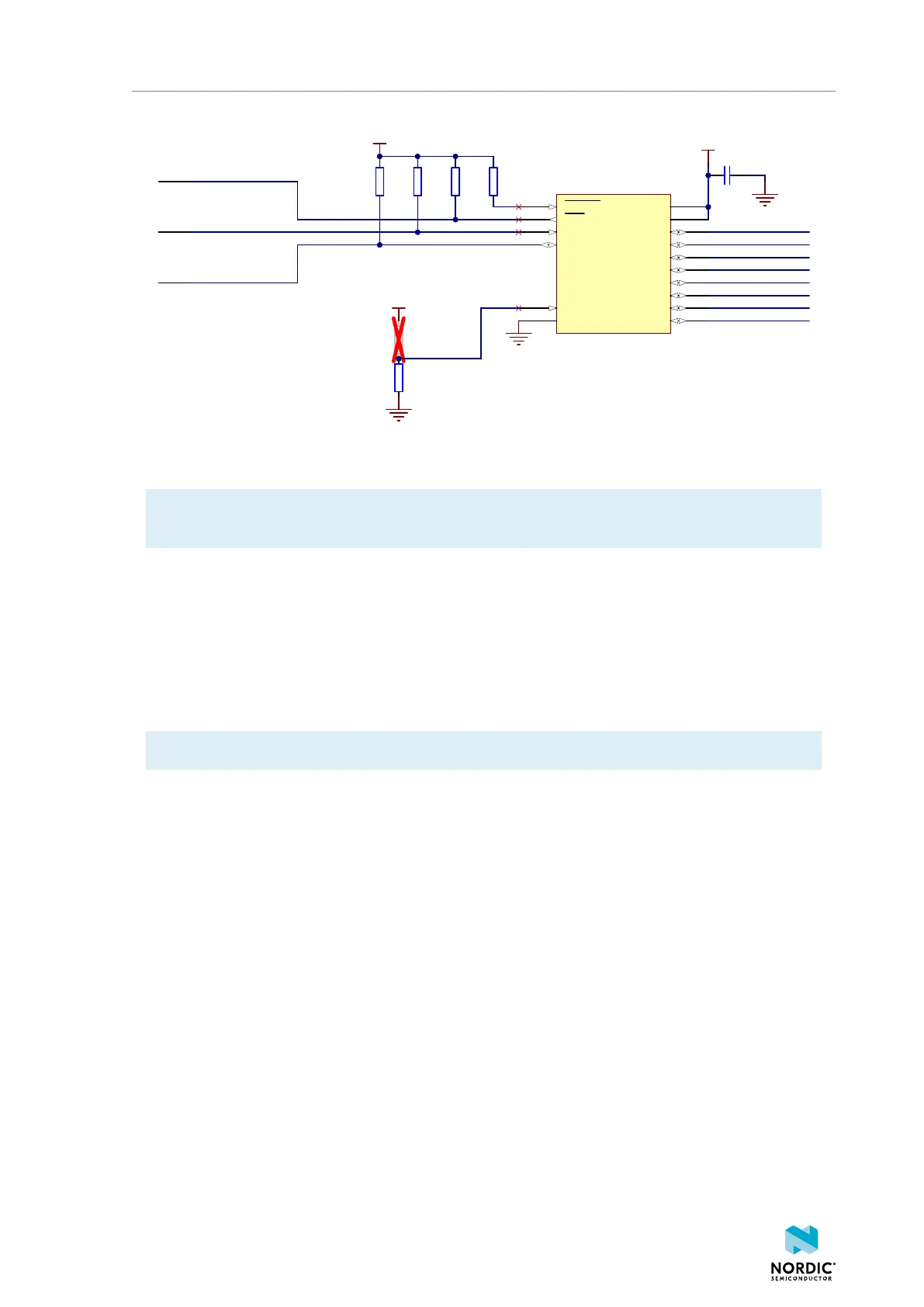
U7
PCAL6408A
I/O expander
7-bit slave address: 0x20
Figure 15: I/O expander schematic
Note: Software debouncing is not needed when using the I/O expander. Each button on the nRF52
DK has a debouncing filter.
4.6 32.768 kHz crystal
The nRF52832 SoC can use an optional 32.768 kHz crystal (X2) for higher accuracy and lower average
power consumption.
On the nRF52 DK, P0.00 and P0.01 are used for the 32.768 kHz crystal by default and are not available
as GPIO on the connectors.
Note: When using ANT/ANT+, the 32.768 kHz crystal (X2) is required for correct operation.
If P0.00 and P0.01 are needed as normal I/Os, then the 32.768 kHz crystal can be disconnected and the
GPIO routed to the connectors. Cut the shorting track on SB1 and SB2, and solder SB3 and SB4. See the
following figure for reference.
4397_500
19