Hardware description
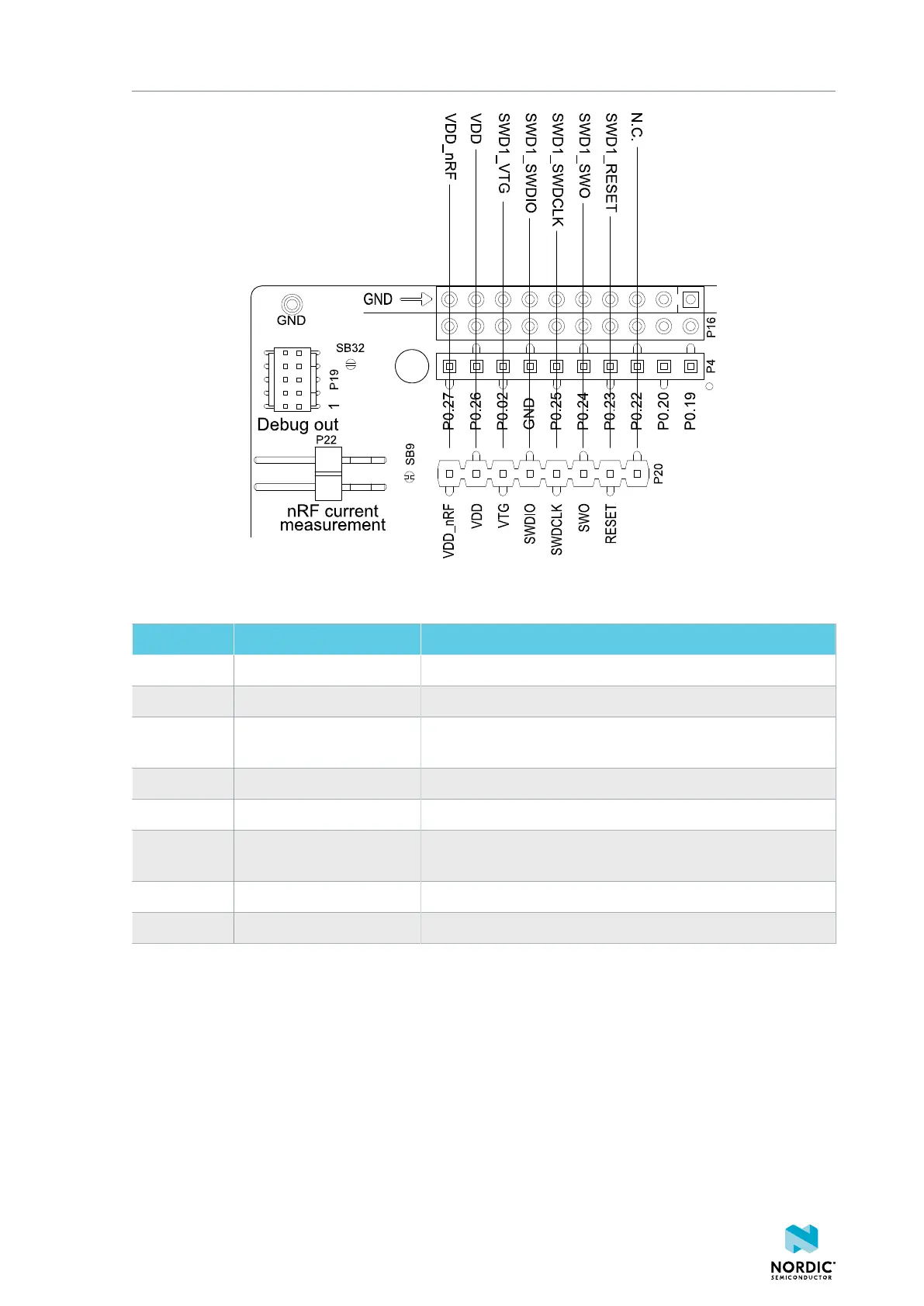
Figure 23: Debug output connector P20
Pin number Signal Description
1 VDD_nRF nRF52832 SoC power domain
2 VDD Main nRF52 DK power domain
3 SWD1_VTG Voltage supply from the external target. Used as enable
signal for activating SWD1.
4 SWD1_SWDIO SWD data line
5 SWD1_SWDIO SWD clock line
6 SWD1_SWO The SWO line is not needed for programming and debugging
over SWD.
7 SWD1_RESET Reset line
8 N.C. Not used
Table 7: Pinout of connector P20 for programming external targets
4.9 NFC antenna interface
The nRF52 DK supports an NFC tag.
NFC-A Listen Mode operation is supported on the nRF52832 SoC. The NFC antenna input is available on
connector P23 on the nRF52 DK.
4397_500
25