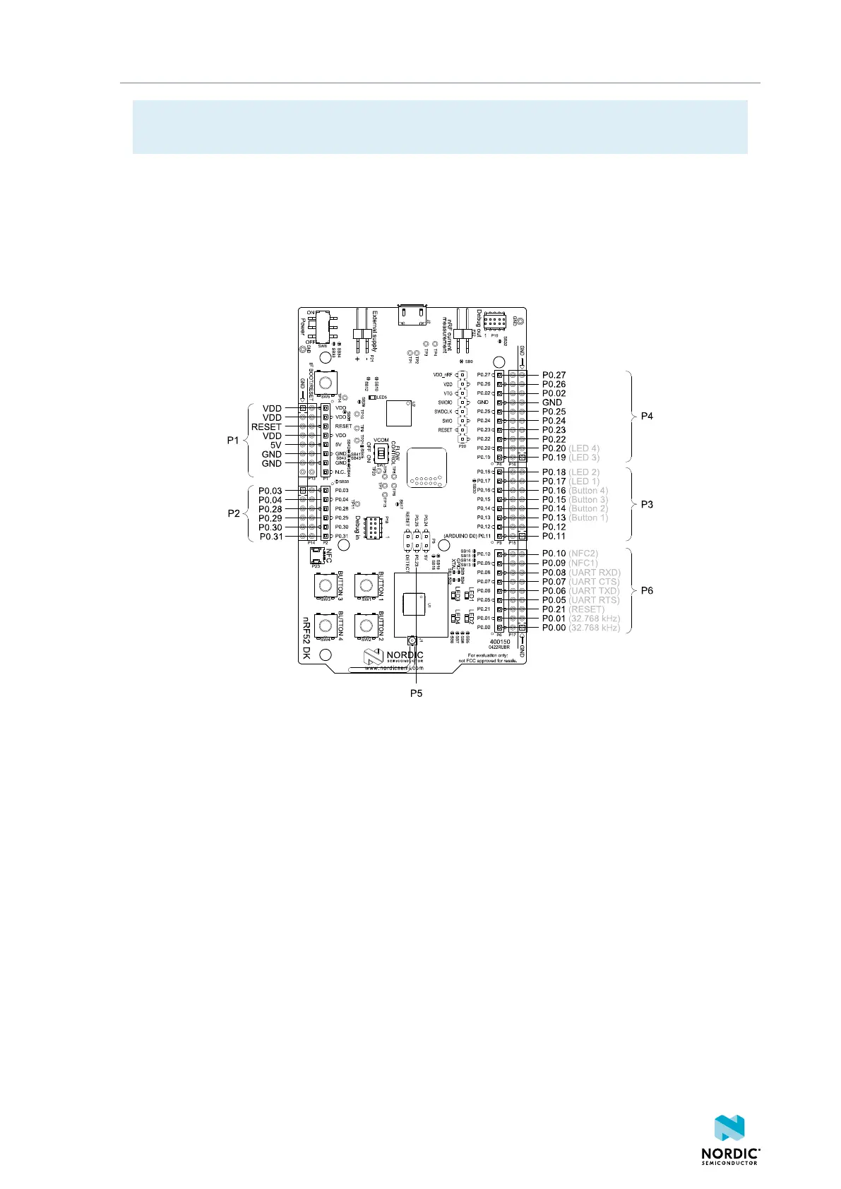
Hardware description
Note: Connect only one power source at a time. Shorting the solder bridges removes the reverse
voltage protection.
4.4 Connector interface
Access to the nRF52832 General-Purpose Input/Output (GPIO)s is available from connectors P2, P3, P4, P5,
and P6.
The P1 connector provides access to ground and power on the nRF52 DK.
Figure 10: nRF52 DK connectors
Some of the signals are also available on connectors P7, P8, P9, P10, P11, and P12, located on the back
side of the DK. By mounting pin lists on the connector footprints, the nRF52 DK can be used as a shield for
3.3 V Arduino motherboards or other boards that follow the Arduino standard.
For easy access to GPIO, power, and ground, the signals can also be found on the through-hole connectors
P13–P17.
Some pins have default settings:
• P0.00 and P0.01 are used for the 32.768 kHz crystal and are not available on the connectors. See
32.768 kHz crystal on page 19 for more information.
• P0.05, P0.06, P0.07, and P0.08 are used by the UART connected to the interface MCU. See
Virtual serial port on page 8 for more information.
• P0.09 and P0.10 are by default used by signals NFC1 and NFC2. See NFC antenna interface on page
25 for more information.
• P0.13–P0.20 are by default connected to the buttons and LEDs. See Buttons and LEDs on page
16 for more information.
When the nRF52 DK is used as a shield together with an Arduino standard motherboard, the Arduino
signals are routed as shown in the following figure.
4397_500
15