Hardware description
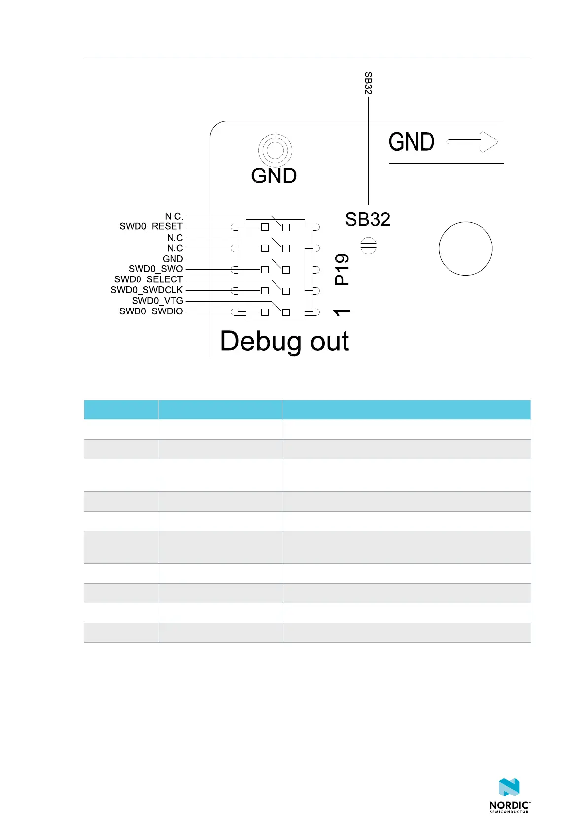
Figure 21: Debug output connector P19
Pin number Signal Description
1 SWD0_VTG Optional voltage supply to the external target
2 SWD0_SWDIO SWD Data Input/Output
3 SWD0_SELECT Debug out select signal. Connect to ground on external
board.
4 SWD0_SWDCLK Serial Wire Clock line
5 GND Ground
6 SWD0_SW0 The Serial Wire Output (SWO) line is not needed for
programming and debugging over SWD.
7 N.C. Not used
8 N.C. Not used
9 N.C. Not used
10 SWD0_RESET Reset line
Table 6: Pinout of connector P19 for programming external targets
4.8.2 Programming a board with custom connections
If your external board has custom connections to programming and debugging pins, use debug output on
connector P20.
Connect the boards as shown in the following figure.
4397_500
23