MPC5746R Hardware Design Guide, Rev. 1
Power Supply
NXP Semiconductors10
3.3 External 1.25 V Supply
If an external regulator is used for the VDD_LV supply, the pass transistor is not required. In this case, the
internal voltage regulator driver should be disabled by setting the REG_SEL bit in the Miscellaneous
Device Configuration Format (DCF) client. This is accomplished via a DCF record programmed into the
UTEST flash memory. See the DCF Chapter of the MPC5746R Reference Manual for complete
information regarding the use of DCF records and UTEST flash memory.
Note that the VRC_CTRL will remain active until the Reset Generation Module (RGM) enters the reset
phase 3, where the UTEST configuration is read. When using an external VDD_LV supply, the
VRC_CTRL pin should be left floating (no connect). See the RGM chapter of the MPC5746R Reference
Manual for more information.
3.4 Input and output pins power supply segmentation
Each I/O pin is associated with one of the power domains. The majority of the I/O pins are powered by the
VDD_HV_IO_MAIN. The VDD_HV_IO_JTAG, VDD_HV_IO_FEC, and VDD_HV_IO_MSC domains
are primarily intended to allow the JTAG, FEC and MSC interfaces to be operated at a voltage level
different from the VDD_HV_IO_MAIN domain if desired. However, they can also be used to power a
limited amount of I/O pins at an alternative voltage level.
The voltage level supplied on any I/O domain determines the output voltage level and input transition
levels for the I/O pins associated with that domain. Each power domain with corresponding I/O pins is
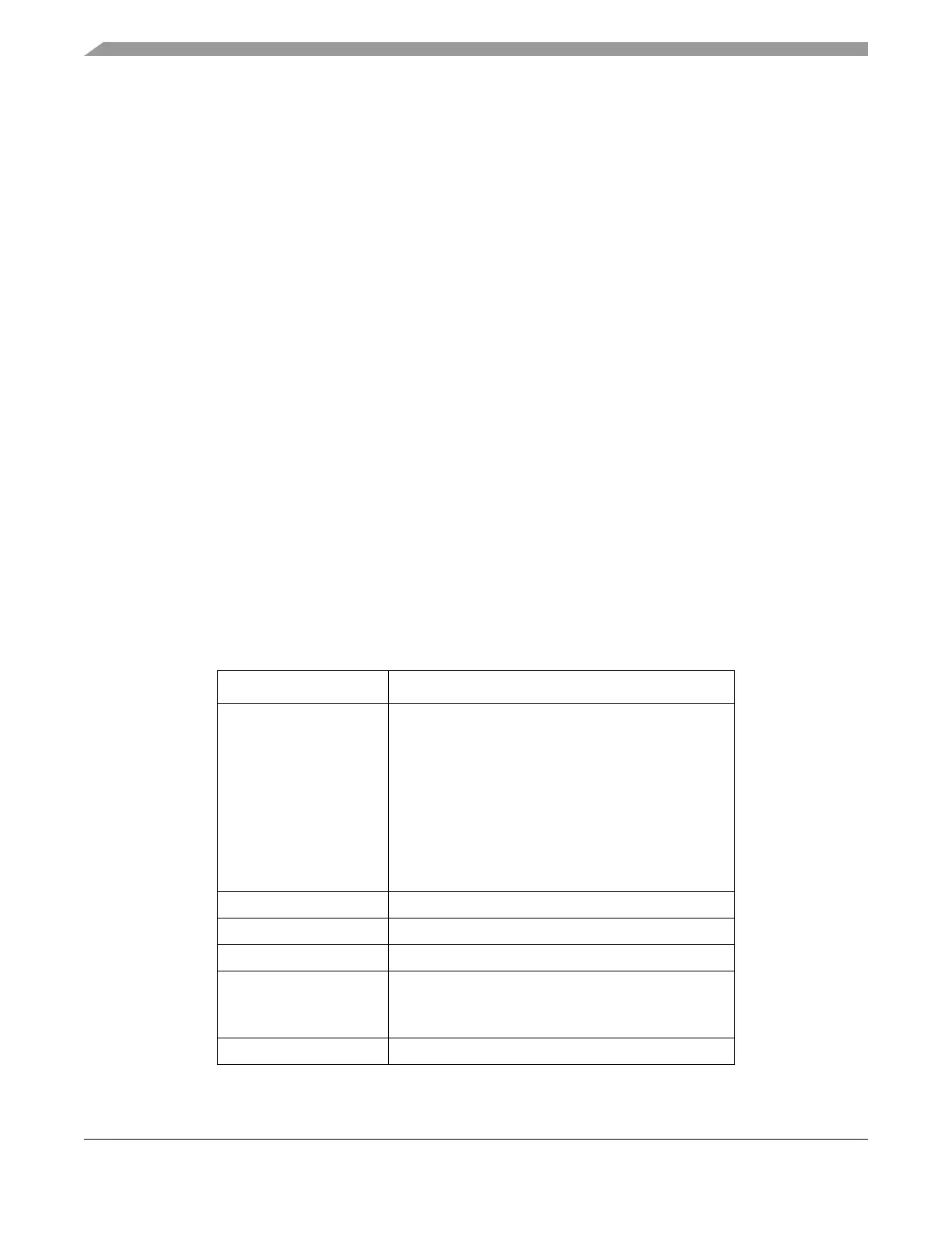
shown in Table 8. Each power domain needs to be maintained below 80 mA. In addition, the sum of all
I/O power domains should be maintained below 200mA as described in the MPC5746R Data Sheet. Note
that, not all of the listed I/O pins are available on some packages.
1
Table 8. Power Domains vs. I/O
Power Domain I/O Pins
VDD_HV_IO_MAIN
PD[0–15]
PE[0]
PF[0–13]
PG[1–7, 9–15]
PH[0–15]
PI[0–5]
PJ[0–15]
PK[0–2, 4–5, 7–14]
PL[0–1]
VDD_HV_IO_JTAG PB[0–1]
VDD_HV_IO_FEC PC[0–13]
VDD_HV_IO_MSC PA[0–13]
VDD_HV_ADV_SAR
PW[0–3]
PX[0–15]
PY[0–15]
VDD_HV_ADV_SD PZ[0–15]

 Loading...


